LT3092
4
3092fc
For more information www.linear.com/LT3092
elecTrical characTerisTics
Note 1: Stresses beyond those listed under Absolute Maximum Ratings
may cause permanent damage to the device. Exposure to any Absolute
Maximum Rating condition for extended periods may affect device
reliability and lifetime.
Note 2: Unless otherwise specified, all voltages are with respect to V
OUT
.
The LT3092E is tested and specified under pulse load conditions such
that T
J
@ T
A
. The LT3092E is 100% tested at T
A
= 25°C. Performance at
–40°C and 125°C is assured by design, characterization, and correlation
with statistical process controls. The LT3092I is guaranteed to meet all
data sheet specifications over the full –40°C to 125°C operating junction
temperature range. The LT3092MP is 100% tested and guaranteed over
the –55°C to 125°C operating junction temperature range.
Note 3: Minimum load current is equivalent to the quiescent current of
the part. Since all quiescent and drive current is delivered to the output
of the part, the minimum load current is the minimum current required to
maintain regulation.
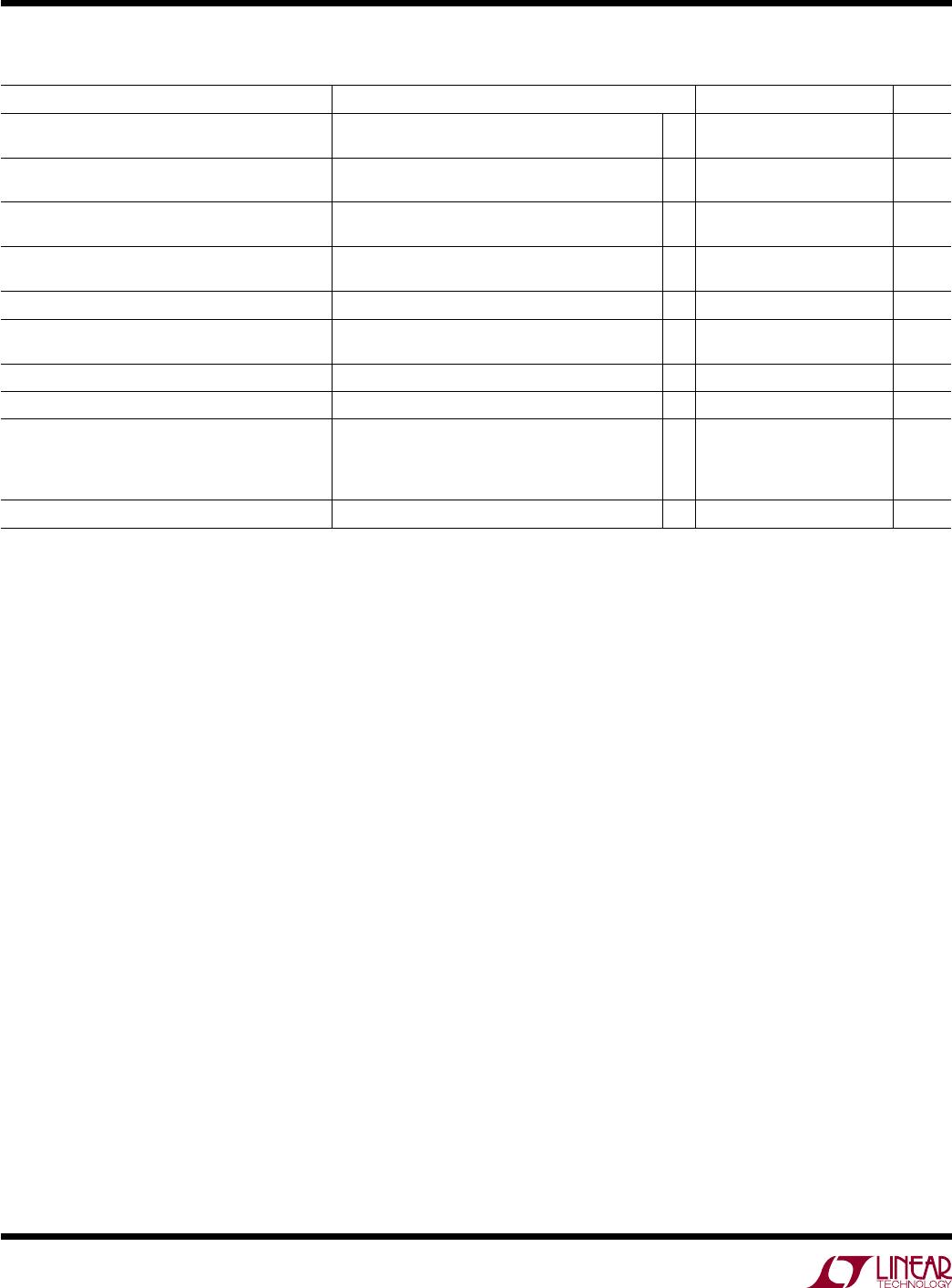
PARAMETER CONDITIONS MIN TYP MAX UNITS
SET Pin Current I
SET
V
IN
= 2V, I
LOAD
= 1mA
2V ≤ V
IN
≤ 40V, 1mA ≤ I
LOAD
≤ 200mA
l
9.9
9.8
10
10
10.1
10.2
µA
µA
Offset Voltage (V
OUT
– V
SET
) V
OS
V
IN
= 2V, I
LOAD
= 1mA
V
IN
= 2V, I
LOAD
= 1mA
l
–2
–4
2
4
mV
mV
Current Regulation (Note 7)
∆I
SET
∆V
OS
∆I
LOAD
= 1mA to 200mA
∆I
LOAD
= 1mA to 200mA
l
–0.1
–0.5
–2
nA
mV
Line Regulation
∆I
SET
∆V
OS
∆V
IN
= 2V to 40V, I
LOAD
= 1mA
∆V
IN
= 2V to 40V, I
LOAD
= 1mA
0.03
0.003
0.2
0.010
nA/V
mV/V
Minimum Load Current (Note 3) 2V ≤ V
IN
≤ 40V
l
300 500 µA
Dropout Voltage (Note 4) I
LOAD
= 10mA
I
LOAD
= 200mA
l
l
1.22
1.3
1.45
1.65
V
V
Current Limit V
IN
= 5V, V
SET
= 0V, V
OUT
= –0.1V
l
200 300 mA
Reference Current RMS Output Noise (Note 5) 10Hz ≤ f ≤ 100kHz 0.7 nA
RMS
Ripple Rejection f = 120Hz, V
RIPPLE
= 0.5V
P-P
, I
LOAD
= 0.1A,
C
SET
= 0.1µF, C
OUT
= 2.2µF
f = 10kHz
f = 1MHz
90
75
20
dB
dB
dB
Thermal Regulation
I
SET
10ms Pulse 0.003 %/W
The l denotes the specifications which apply over the full operating
temperature range, otherwise specifications are at T
J
= 25°C. (Note 2)
Note 4: For the LT3092, dropout is specified as the minimum input-to-
output voltage differential required supplying a given output current.
Note 5: Adding a small capacitor across the reference current resistor
lowers output noise. Adding this capacitor bypasses the resistor shot noise
and reference current noise (see the Applications Information section).
Note 6: Diodes with series 1k resistors clamp the SET pin to the OUT pin.
These diodes and resistors only carry current under transient overloads.
Note 7: Current regulation is Kelvin-sensed at the package.
Note 8: This IC includes overtemperature protection that protects the
device during momentary overload conditions. Junction temperature
exceeds the maximum operating junction temperature when
overtemperature protection is active. Continuous operation above the
specified maximum operating junction temperature may impair device
reliability.