85411 Data Sheet
©2016 Integrated Device Technology, Inc Revision C January 20, 20163
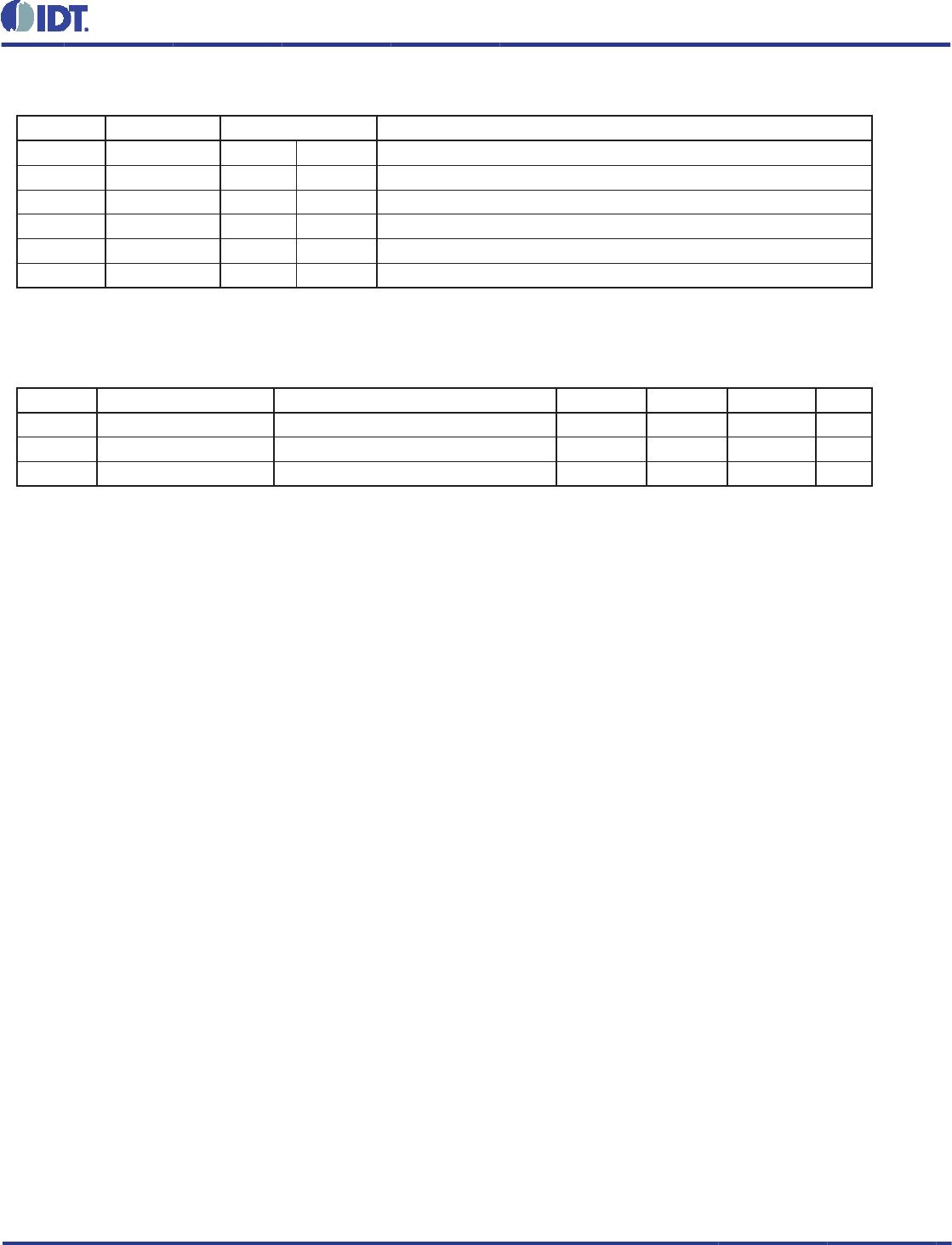
TABLE 3A. POWER SUPPLY DC CHARACTERISTICS, V
DD
= 3.3V±10%, TA = 0°C TO 70°C
TABLE 3B. DIFFERENTIAL DC CHARACTERISTICS, V
DD
= 3.3V±10%, TA = 0°C TO 70°C
Symbol Parameter Test Conditions Minimum Typical Maximum Units
V
DD
Positive Supply Voltage 2.97 3.3 3.63 V
I
DD
Power Supply Current 50 mA
NOTE: Stresses beyond those listed under Absolute
Maximum Ratings may cause permanent damage to the
device. These ratings are stress specifi cations only. Functional
operation of product at these conditions or any conditions beyond
those listed in the DC Characteristics or AC Characteristics is not
implied. Exposure to absolute maximum rating conditions for ex-
tended periods may affect product reliability.
TABLE 3C. LVDS DC CHARACTERISTICS, V
DD
= 3.3V±10%, TA = 0°C TO 70°C
Symbol Parameter Test Conditions Minimum Typical Maximum Units
V
OD
Differential Output Voltage 247 325 454 mV
Δ V
OD
VOD Magnitude Change 0 50 mV
V
OS
Offset Voltage 1.325 1.45 1.575 V
Δ V
OS
VOS Magnitude Change 5 50 mV
I
OFF
Power Off Leakage -20 ±1 +20 µA
I
OSD
Differential Output Short Circuit Current -3.5 -5 mA
I
OS
Output Short Circuit Current -3.5 -5 mA
ABSOLUTE MAXIMUM RATINGS
Supply Voltage, V
DD
4.6V
Inputs, V
I
-0.5V to V
DD
+ 0.5V
Outputs, I
O
Continuous Current 10mA
Surge Current 15mA
Package Thermal Impedance, θ
JA
112.7°C/W (0 lfpm)
Storage Temperature, T
STG
-65°C to 150°C
Symbol Parameter Test Conditions Minimum Typical Maximum Units
I
IH
Input High Current
CLK V
DD
= V
IN
= 3.63V 5 µA
nCLK V
DD
= V
IN
= 3.63V 150 µA
I
IL
Input Low Current
CLK V
DD
= 3.63, V
IN
= 0V -150 µA
nCLK V
DD
= 3.63V, V
IN
= 0V -5 µA
V
PP
Peak-to-Peak Input Voltage; NOTE 1 0.15 1.3 V
V
CMR
Common Mode Input Voltage; NOTE 1, 2 0.5 V
DD
- 0.85 V
NOTE 1: V
IL
should not be less than -0.3V.
NOTE 2: Common mode voltage is defi ned as V
IH
.