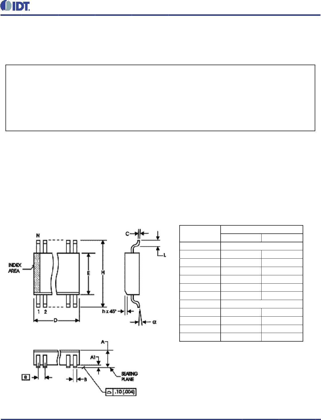
85411 Data Sheet
©2016 Integrated Device Technology, Inc Revision C January 20, 201611
POWER CONSIDERATIONS
This section provides information on power dissipation and junction temperature for the 85411.
Equations and example calculations are also provided.
1. Power Dissipation.
The total power dissipation for the 85411 is the sum of the core power plus the power dissipated in the load(s).
The following is the power dissipation for V
DD
= 3.3V + 10% = 3.63V, which gives worst case results.
• Power (core)
MAX
= V
DD_MAX
* I
DD_MAX
= 3.63V * 50mA = 181.5mW
2. Junction Temperature.
Junction temperature, Tj, is the temperature at the junction of the bond wire and bond pad and directly affects the reliability of the
device. The maximum recommended junction temperature for HiPerClockS
TM
devices is 125°C.
The equation for Tj is as follows: Tj = θJA * Pd_total + TA
Tj = Junction Temperature
θ
JA = Junction-to-Ambient Thermal Resistance
Pd_total = Total Device Power Dissipation (example calculation is in section 1 above)
T
A
= Ambient Temperature
In order to calculate junction temperature, the appropriate junction-to-ambient thermal resistance θ
JA
must be used. Assuming a
moderate air fl ow of 200 linear feet per minute and a multi-layer board, the appropriate value is 103.3°C/W per Table 5 below.
Therefore, Tj for an ambient temperature of 70°C with all outputs switching is:
70°C + 0.182W * 103.3°C/W = 88.8°C. This is below the limit of 125°C.
This calculation is only an example. Tj will obviously vary depending on the number of loaded outputs, supply voltage, air fl ow, and the
type of board (multi-layer).
TABLE 5. THERMAL RESISTANCE θ
JA
FOR 8-LEAD SOIC, FORCED CONVECTION
θ
JA
by Velocity (Linear Feet per Minute)
0 200 500
Single-Layer PCB, JEDEC Standard Test Boards 153.3°C/W 128.5°C/W 115.5°C/W
Multi-Layer PCB, JEDEC Standard Test Boards 112.7°C/W 103.3°C/W 97.1°C/W
NOTE: Most modern PCB designs use multi-layered boards. The data in the second row pertains to most designs.