AD421
9
REV. C
The HC11 generates the requisite eight clock pulses with data
valid on the rising edges. After the MSBY is transmitted, the
least significant byte (LSBY) is loaded from memory and
transmitted in a similar fashion. To complete the transfer, the
LATCH pin is driven high when loading the complete 16-bit
word into the AD421.
AD421 TO MICROWIRE INTERFACE
The flexible serial interface of the AD421 is also compatible
with the National Semiconductor MICROWIRE interface. The
MICROWIRE interface is used in microcontrollers such as the
COP400 and COP800 series of processors. A generic interface
to use the MICROWIRE interface is shown in Figure 9. The
G1, SK, and SO pins of the MICROWIRE interface respec-
tively connect to the LATCH, CLOCK, and DATA IN pins of
the AD421.
SK
SO
CLOCK
DATA IN
LATCH
AD421*
MICROWIRE
* ADDITIONAL PINS OMITTED FOR CLARITY
G1
Figure 9. AD421 to MICROWIRE Interface
Opto-Isolated Interface
The AD421 has a versatile serial 3-wire serial interface making
it ideal for minimizing the number of control lines required for
isolation of the digital system from the control loop. In intrinsi-
cally safe applications or due to noise, safety requirements, or
distance, it may be necessary to isolate the AD421 from the
controller. This can easily be achieved by using opto-isolators.
Figure 10 shows an opto-isolated interface to the AD421 where
CLOCK, DATAIN and LATCH are driven from opto-couplers.
Be aware of signal inversion across the opto-couplers. If opto-
couplers with relatively slow rise and fall times are used, Schmitt
triggers may be required on the digital inputs to prevent errone-
ous data being presented to the DAC.
0.1F2.2F
V
CC
10k
V
CC
10k
V
CC
10k
V
CC
CLOCK
LATCH
DATA IN
AD421*
COM
CLOCK
LATCH
DATA IN
V
CC
* ADDITIONAL PINS OMITTED FOR CLARITY
Figure 10. Opto-Isolated Interface
APPLICATIONS SECTION
Basic Operating Configuration
Figure 11 shows the basic connection diagram for the AD421
operating at 5 V. This circuit shows the minimum of external
components to operate the AD421. In the diagram, the AD421’s
regulator loop in conjunction with the DN25D pass transistor
provides the V
CC
voltage for the AD421 itself and for other
devices in the transmitter. The V
CC
pin should be well decou-
pled with a 2.2 µF capacitor to ensure regulator stability and to
absorb power glitches on the V
CC
line of the AD421 and other
devices in the system. If the AD421 is operated with V
CC
= 3 V,
the transfer function shifts negative. To correct for this a 16 k
resistor connected between COM and LOOPRTN will approxi-
mately compensate for the V
CC
supply sensitivity in moving from
5 V to 3 V by adjusting the gain of the AD421.
C1 C2 C3COM
COM TO EXTERNAL
CIRCUITRY
V
CC
LV
2.2F
COM
V
CC
TO EXTERNAL
CIRCUITRY
DN25D
DRIVE
COMP
0.01F
1k
1000pF
BOOST
LOOP RTN
V
LOOP
0.01F0.01F
0.0033F
LATCH
CLOCK
DATA
REF IN
REF OUT2 REF OUT1
4.7F
COM
AD421
Figure 11. Basic Connection Diagram
AD421
10
REV. C
A capacitor of 0.01 µF connected between COMP and DRIVE
is required to stabilize the feedback loop formed with the
regulator op amp and the external pass transistor. An external
snubber circuit of 1 k and 1000 pF is required between the
DRIVE pin and COM and a 0.1 µF cap between COMP and
DRIVE to stabilize the feedback loop formed by the regulator
op amp and the external pass transistor.
The internal 2.5 V reference on the AD421 is used as the refer-
ence for the AD421 and this has to be decoupled with a 4.7 µF
capacitor for compensation and stability purposes. The sigma-
delta DAC on the part consists of a second order modulator
followed by a continuous time filter. The resistors for each of
the filter sections are on-chip while the capacitors are external
on the C1 to C3 pins. To meet the specified full-scale settling
on the part, low dielectric absorption capacitors (NPO) are
required. Suitable values for these capacitors are C1 = C2 =
0.01 µF, and C3 = 0.0033 µF.
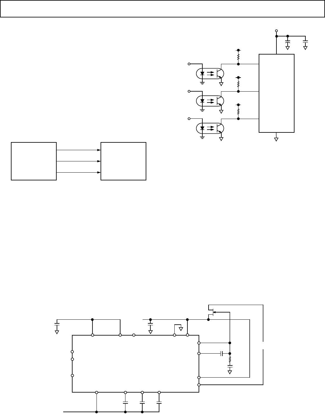
The digital interface on the AD421 consists of just three wires:
DATA, CLOCK and LATCH. The interface connects directly
to the serial ports of commonly-used microcontrollers without
the need for any external glue logic. Data is loaded into an input
shift register on the rising edge of the CLOCK signal and is
transferred to the DAC latch on the rising edge of the LATCH
signal.
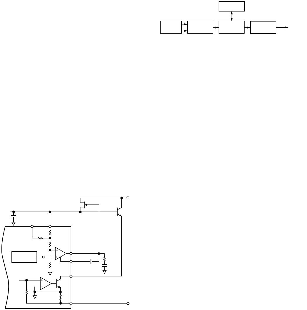
Reduce Power Load on External FET
Figure 12 shows a circuit where an external NPN transistor is
added to reduce the power loading on the FET. The FET will
supply the V
CC
and an external high voltage NPN bipolar tran-
sistor can carry the BOOST current. The BOOST pin sinks the
necessary current from the loop so that the current flowing into
BOOST plus the current flowing into COM is equal to the
programmed loop current. The external NPN transistor reduces
the external power load that the FET has to carry to less than
750 µA if no other components share the V
CC
line and to less
than 4 mA in applications that share the same V
CC
line as the
AD421.
1.21V
112.5k
134k
75k
121k
V
CC
LV
2.2F
COM
V
CC
TO EXTERNAL
CIRCUITRY
DN25D
DRIVE
COMP
0.01F
1k
1000pF
LOOP(+)
BANDGAP
REFERENCE
AD421
BC639/BC337
BOOST
40
80k
LOOP RTN
LOOP(–)
Figure 12. External NPN Transistor Reduces Power Load
on FET
Smart Transmitter
The AD421 is intended for use in 4 mA to 20 mA smart trans-
mitters. A smart transmitter is a system that incorporates a
microprocessor system which is used for linearization and
communication. Figure 13 shows a block diagram of a typical
smart transmitter. In this example, the transmitter does not have
any digital communication capabilities.
4mA TO 20mA
MEASUREMENT
CIRCUIT
MICRO-
PROCESSOR
D/A
CONVERTER
A/D
CONVERTER
MEMORY
SENSORS
Figure 13. Typical Smart Transmitter
Figure 14 shows a typical smart transmitter application circuit
using the AD421.
The sensor voltage to be measured at the transmitter is con-
verted using a high resolution sigma-delta converter such as
the AD7714 or AD7715. These devices have an on-board PGA
which can provide gains on the analog front end from 1 to 128.
This allows for an analog input range as low as 10 mV which
allows the transducer to be connected directly to the ADC. The
AD7714/AD7715 have digital calibration techniques which are
used to eliminate gain and offset errors. In addition, back-
ground calibration techniques are provided whereby the part
continually calibrates itself and the user does not have to
worry about issuing periodic calibration commands to remove
effects of time and temperature drift.
In normal operation the microprocessor reads the data from the
AD7714/AD7715. After the data is processed by the micro-
controller, the data is transferred from the serial port of the
processor to the AD421 for transmission over the 4 to 20 mA
loop back to the control center.
The AD421 regulates the loop voltage to create power for the
rest of the transmitter circuitry. In Figure 14, the derived V
CC
voltage is 3.3 V which is achieved by connecting the LV pin to
V
CC
through 0.01 µF. REF OUT2 provides the reference volt-
age for the AD421 itself while REF OUT1 provides the refer-
ence voltage for the AD7714/AD7715.
AD421
11
REV. C
DV
DD
AV
DD
REF IN
CS
DATA OUT
SCLK
DATA IN
AGND
DGND
MCLK IN
MCLK OUT
AD7714/
AD7715
ANALOG
TO
DIGITAL
CONVERTER
SENSORS
RTD
mV TC
4.7F
REF OUT1
BOOST
V
CC
LV
COMP
DRIVE
LOOP
RTN
REF OUT2
REF IN
CLOCK
LATCH
DATA
COM
C1 C2
C3
LOOP
POWER
0.01F
DN25D
2.2F
3.3V
1.25V
4.7F
AMBIENT
TEMP
SENSOR
AD421
MICROCONTROLLER
V
CC
GND
0.01F
1k
1000pF
0.1F
100k
Figure 14. AD421 in Smart Transmitter Application
Figure 16 shows a block diagram of a smart and intelligent
transmitter. An intelligent transmitter is a transmitter in which
the functions of the microprocessor are shared between deriving
the primary measurement signal, storing information regarding
the transmitter itself, its application data and its location and
also managing a communication system which enables two way
communication to be superimposed on the same circuit that
carries the measurement signal. A smart transmitter incorporat-
ing the HART protocol is an example of a smart intelligent
transmitter.
4mA TO 20mA
MEASUREMENT
CIRCUIT
MICRO-
PROCESSOR
D/A
CONVERTER
A/D
CONVERTER
MEMORY
SENSORS
COMMUNICATION
SYSTEM
Figure 16. Smart and Intelligent Transmitter
Figure 17 shows an example of the AD421 in a HART transmit-
ter application. Most of the circuit is as outlined in the smart
transmitter as shown in Figure 14. The HART data transmitted
on the loop is received by the transmitter using a bandpass filter
and modem and the HART data is transferred to the micro-
controller’s UART or asynchronous serial port. HART data to
be transmitted on the loop is sent from the microcontroller’s
UART or asynchronous serial port to the modem. It is then
waveshaped before being coupled onto the AD421’s output at
the C3 pin. The value of the coupling capacitor C
C
is determined
by the waveshaper output and the C3 capacitor of the AD421. The
blocks containing the Bell 202 Modem, waveshaper and bandpass
filter come in a complete solution with the 20C15 from Symbios
Logic, Inc., or HT2012 from SMAR Research Corp.
For a more complete AD421-20C15 interface, please refer to
Application Note AN-534 on the Analog Devices’ website
www.analog.com or contact your local sales office.
HART Interfacing
The HART protocol uses a frequency shift (FSK) keying tech-
nique based on the Bell 202 Communication Standard which is
one of several standards used to transmit digital signals over
the telephone lines. This technique is used to superimpose
digital communication on to the 4 mA to 20 mA current loop
connecting the central system to the transmitter in the field.
Two different frequencies, 1200 Hz and 2200 Hz, are used to
represent binary 1 and 0 respectively, as shown in Figure 15.
These sine wave tones are superimposed on the dc signal at a
low level with the average value of the sine wave signal being
zero. This allows simultaneous analog and digital communica-
tions. Additionally, no dc component is added to the existing
4 mA to 20 mA signal regardless of the digital data being sent
over the line. Consequently, existing analog instruments con-
tinue to work in systems that implement HART as the low-pass
filtering usually present effectively removes the digital signal. A
single pole 10 Hz low-pass filter effectively reduces the commu-
nication signal to a ripple of about ± 0.01% of the full-scale
signal. The HART protocol specifies that master devices like a
host control system or a hand held terminal transmit a voltage
signal whereas a slave or field device transmits a current signal.
The current signal is converted into a corresponding voltage by
the loop load resistor.
APPROX
+0.5mA
APPROX
0.5mA
1200Hz
1
2200Hz
0
Figure 15. HART Transmission of Digital Signals

AD421BNZ

Mfr. #:
Manufacturer:
Analog Devices Inc.
Description:
Digital to Analog Converters - DAC IC 16-BIT
Lifecycle:
New from this manufacturer.
Delivery:
DHL FedEx Ups TNT EMS
Payment:
T/T Paypal Visa MoneyGram Western Union