LT3007 Series
13
3007fa
For more information www.linear.com/LT3007
APPLICATIONS INFORMATION
layer GND planes achieves 45°C/W thermal resistance.
This is approximately a 30% improvement over the lowest
numbers shown in Table 3.
Thermal Considerations
The LT3007’s maximum rated junction temperature of
125°C limits its power-handling capability. Two compo
-
nents comprise the power dissipated by the device:
1. Output current multiplied by the input/output voltage
differential: I
OUT
• (V
IN
– V
OUT
)
2. GND pin current multiplied by the input voltage:
I
GND
• V
IN
GND pin current is found by examining the GND Pin Cur-
rent cur
ves in the Typical Performance Characteristics
section.
Power dissipation is equal to the sum of the two
components listed prior.
The LT3007 regulator has internal thermal limiting designed
to protect the device during overload conditions. For con
-
tinuous normal
conditions, do not exceed the maximum
junction temperature rating of 125°C. Carefully consider
all sources of thermal resistance from junction to ambi
-
ent including other heat sources mounted in proximity to
the LT3007. For surface mount devices, heat sinking is
accomplished by
using the heat spreading capabilities of
the PC board and its copper traces. Copper board stiffen-
ers and
plated through-holes can also be used to spread
the heat generated by power devices.
The following tables list thermal resistance for several
different board sizes and copper areas. All measurements
were taken in still air on 3/32" FR-4 two-layer boards with
one ounce copper.
PCB layers, copper weight, board layout and thermal vias
affect the resultant thermal resistance. Although Table2
provides thermal resistance numbers for 2-layer boards
with 1 ounce copper, modern multilayer PCBs provide bet
-
ter performance than found in these tables. For example,
a 4-layer, 1 ounce copper PCB board with three thermal
vias from the three fused TSOT-23 GND pins to inner
Table 3: Measured Thermal Resistance for TSOT-23 Package
COPPER AREA
BOARD
AREA
THERMAL RESIST
ANCE
(JUNCTION-TO-AMBIENT)TOPSIDE* BACKSIDE
2500mm
2
2500mm
2
2500mm
2
65°C/W
1000mm
2
2500mm
2
2500mm
2
67°C/W
225mm
2
2500mm
2
2500mm
2
70°C/W
100mm
2
2500mm
2
2500mm
2
75°C/W
50mm
2
2500mm
2
2500mm
2
85°C/W
*Device is mounted on the topside.
Calculating Junction Temperature
Example: Given an output voltage of 3.3V, an input volt-
age range
of 12V ±5%, an output current range of 0mA
to
20mA and a maximum ambient temperature of 85°C,
what will the maximum junction temperature be?
The power dissipated by the device is equal to:
I
OUT(MAX)
(V
IN(MAX)
– V
OUT
) + I
GND
(V
IN(MAX)
)
where,
I
OUT(MAX)
= 20mA
V
IN(MAX)
= 12.6V
I
GND
at (I
OUT
= 20mA, V
IN
= 12.6V) = 0.3mA
So,
P = 20mA(12.6V – 3.3V) + 0.3mA(12.6V) = 189.8mW
The thermal resistance ranges from 65°C/W to 85°C/W
depending on the copper area. So, the junction temperature
rise above ambient approximately equals:
0.1898W(75°C/W) = 14.2°C
LT3007 Series
14
3007fa
For more information www.linear.com/LT3007
The maximum junction temperature equals the maximum
junction temperature rise above ambient plus the maximum
ambient temperature or:
T
J(MAX)
= 85°C + 14.2°C = 99.2°C
High Temperature Operation
Care must be taken when designing LT3007 applications to
operate at high ambient temperatures. The LT3007 works
at elevated temperatures but erratic operation can occur
due to unforeseen variations in external components.
Some tantalum capacitors are available for high tempera
-
ture operation,
but ESR is often several Ohms; capacitor
ESR aboveis unsuitable for use with the LT3007.
Ceramic capacitor manufacturers (Murata, AVX, TDK,
and Vishay at the time of this writing) now offer ceramic
capacitors that are rated to 150°C using an X8R dielectric.
Device instability will occur if the output capacitor value
and ESR are outside design limits at elevated tempera
-
ture and operating
DC voltage bias (see information on
capacitor characteristics under Output Capacitance and
Transient Response). Check each passive component
for absolute value and voltage ratings over the operating
temperature range.
APPLICATIONS INFORMATION
Operation of the LT3007 at temperatures above 125°C
requires careful selection of external components to
ensure output regulation, stability and optimal transient
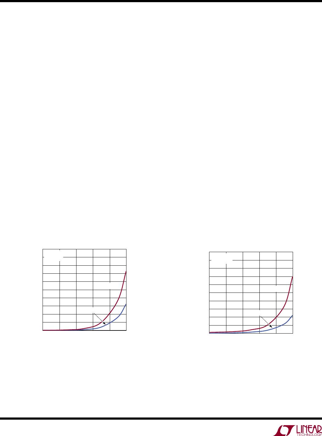
response. Figures 9 and 10 have curves showing power
device leakage (from IN
to OUT) for the LT3007 in both
active
and shutdown states. The minimum external load
must be greater than this leakage to prevent the OUT pin
from rising out of regulation due to power device leakage.
Power device leakage decreases if the LT3007 is active;
if IN is tied directly to SHDN, the minimum required load
is reduced. The recommended minimum external load is
20µA. The use of a feedforward capacitor is required for
operation at temperatures above 135°C (see Feedforward
Capacitance section). For output voltages of 1.2V and
above, the feedforward capacitor ensures good transient
response. Use of the LT3007 at temperatures above 135°C
and output voltages under 1.2V is not advised.
Leakage in capacitors, or from solder flux left after insuf
-
ficient board
cleaning, adversely affects the low quiescent
current
operation. Consider junction temperature increase
due to power dissipation in both the junction and nearby
components to ensure maximum specifications are not
violated for the LT3007 or external components.
Figure 9. Power Device Leakage, SHDN = 0V
Figure 10. Power Device Leakage, SHDN = 1.5V
TEMPERATURE (°C)
100
POWER DEVICE LEAKAGE (μA)
10
1
9
7
5
3
8
6
4
2
0
3007 F09
150120 140110 130
V
OUT
= 0V
V
ADJ
= 0V
V
IN
= 45V
V
IN
= 2.1V
TEMPERATURE (°C)
100
POWER DEVICE LEAKAGE (μA)
2.0
0.2
1.8
1.4
1
0.6
1.6
1.2
0.8
0.4
0
3007 F10
150120 140110 130
V
OUT
= 0V
V
ADJ
= 0.7V
V
IN
= 45V
V
IN
= 2.1V
LT3007 Series
15
3007fa
For more information www.linear.com/LT3007
Figure 11. Reverse-Output Current
OUTPUT AND ADJ VOLTAGE (V)
0
60
80
100
8
40
20
50
70
90
30
10
0
21
43
6 7 9
5
10
3007 F11
REVERSE CURRENT (µA)
OUT CURRENT
ADJ CURRENT
Protection Features
The LT3007 incorporates several protection features that
make it ideal for use in battery-powered circuits. In ad
-
dition to the normal protection features associated with
monolithic regulators, such as current limiting and thermal
limiting, the device also protects against reverse-input
voltages, reverse-output voltages and reverse output-to-
input voltages.
Current limit protection and thermal overload protection
protect the device against current overload conditions at
the output of the device. For normal operation, do not ex
-
ceed a
junction temperature of 125°C. The typical thermal
shutdown cir
cuitry temperature threshold is 160°C.
The IN pin withstands reverse voltages of 50V. The de
-
vice limits current flow to less than 30µA (typically less
than1µA) and no negative voltage appears at OUT. The
device protects both itself and the load against batteries
that are plugged in backwards.
The SHDN pin cannot be driven below GND unless tied to
the IN pin. If the SHDN pin is driven below GND while IN
is powered, the output will turn on. SHDN pin logic cannot
be referenced to a negative rail.
APPLICATIONS INFORMATION
The LT3007 incurs no damage if OUT is pulled below
ground. If IN is left open circuit or grounded, OUT
can be
pulled below ground by 50V. No current flows from the
pass transistor connected to OUT. However, current flows
in (but is limited by) the resistor divider that sets output
voltage. Current flows from the bottom resistor in the
divider and from the ADJ pin’s internal clamp through the
top resistor in the divider to the external circuitry pulling
OUT below ground. If IN is powered by a voltage source,
OUT sources current equal to its current limit capability
and the LT3007 protects itself by thermal limiting if neces
-
sary. In this case, grounding the SHDN
pin turns off the
LT3007 and stops OUT from sourcing current.
The LT3007 incurs no damage if the ADJ pin is pulled
above or below ground by 50V. If IN is left open circuit or
grounded, ADJ acts like a 100k resistor in series with a
diode when pulled above or below ground.
In circuits where a backup battery is required, several
different input/output conditions can occur. The output
voltage may be held up while the input is either pulled
to ground, pulled to some intermediate voltage or is left
open circuit. Current flow back into the output
follows the
cur
ve shown in Figure 11.

LT3007ETS8-1.2#TRMPBF

Mfr. #:
Manufacturer:
Analog Devices / Linear Technology
Description:
LDO Voltage Regulators 3Ua Iq, 20mA, 45V Low Dropout Fault Tolerant Linear Regulators
Lifecycle:
New from this manufacturer.
Delivery:
DHL FedEx Ups TNT EMS
Payment:
T/T Paypal Visa MoneyGram Western Union