LT3007 Series
4
3007fa
For more information www.linear.com/LT3007
PARAMETER CONDITIONS MIN TYP MAX UNITS
Quiescent Current (Notes 6, 7) I
LOAD
= 0µA (E-, I-Grades)
I
LOAD
= 0µA (H-Grade)
l
l
3 6
7
µA
µA
GND Pin Current
V
IN
= V
OUT(NOMINAL)
+ 0.5V (Notes 6, 7)
I
LOAD
= 0µA (E-, I-Grades)
I
LOAD
= 0µA (H-Grade)
I
LOAD
= 100µA (E-, I-Grades)
I
LOAD
= 100µA (H-Grade)
I
LOAD
= 1mA
I
LOAD
= 10mA
I
LOAD
= 20mA
l
l
l
l
l
l
l
3
6
21
160
350
6
7
12
14
50
500
1200
µ
A
µA
µA
µA
µA
µA
µA
Output
V
oltage Noise (Note 9) C
OUT
= 2.2µF, I
LOAD
= 20mA, BW = 10Hz to 100kHz 92 µV
RMS
ADJ Pin Bias Current –10 0.4 10 nA
Shutdown Threshold V
OUT
= Off to On
V
OUT
= On to Off
l
l
0.25
0.67
0.61
1.5 V
V
SHDN Pin Current V
SHDN
= 0V, V
IN
= 45V
V
SHDN
= 45V, V
IN
= 45V
l
l
0.65
±1
2
µA
µA
Quiescent Current in Shutdown V
IN
= 6V, V
SHDN
= 0V (E-, I-Grades)
V
IN
= 6V, V
SHDN
= 0V (H-Grade)
l
l
<1
<9
µA
µA
Ripple Rejection (Note 3) V
IN
– V
OUT
= 2V, V
RIPPLE
= 0.5V
P-P
,
f
RIPPLE
= 120Hz, I
LOAD
= 20mA
LT3007
LT3007-1.2
LT3007-1.5
LT3007-1.8
LT3007-2.5
LT3007-3.3
LT3007-5
58
54
53
52
49
47
42
70
66
65
64
61
59
54
dB
dB
dB
dB
dB
dB
dB
Current
Limit (Note 3) V
IN
= 45V, V
OUT
= 0
V
IN
= V
OUT(NOMINAL)
+ 1V, ∆V
OUT
= –5%
l
22
75 mA
mA
Input Reverse-Leakage Current V
IN
= –45V, V
OUT
= 0
l
1 30 µA
Reverse-Output Current V
OUT
= 1.2V, V
IN
= 0 0.6 10 µA
Note 1: Stresses beyond those listed under Absolute Maximum Ratings
may cause permanent damage to the device. Exposure to any Absolute
Maximum Rating condition for extended periods may affect device
reliability and lifetime.
Note 2: The LT3007 is tested and specified under pulse load conditions
such that T
J
@ T
A
. The LT3007E regulators are 100% tested at T
A
= 25°C
and performance is guaranteed from 0°C to 125°C. Performance at
−40°C to 125°C is assured by design, characterization and correlation
with statistical process controls. The LT3007I regulators are guaranteed
over the full −40°C to 125°C operating junction temperature range.
The LT3007H regulator is 100% tested at the 150°C operating junction
temperature. High junction temperatures degrade operating lifetimes.
Operating lifetime is derated at junction temperature greater than 125°C.
H-grade is available only in the adjustable version
.
Note 3:
The LT3007 adjustable version is tested and specified for these
conditions with the ADJ pin connected to the OUT pin.
Note 4: Operating conditions are limited by maximum junction
temperature. The regulated output voltage specification will not apply
for all possible combinations of input voltage and output current. When
operating at the maximum input voltage, the output current range must be
limited. When operating at the maximum output current, the input voltage
must be limited.
Note 5: Dropout voltage is the minimum input to output voltage differential
needed to maintain regulation at a specified output current. In dropout,
the output voltage equals (V
IN
– V
DROPOUT
). For the LT3007-1.2 and
LT3007-1.5, dropout voltage will be limited by the minimum input voltage.
Note 6: To satisfy minimum input voltage requirements, the LT3007
adjustable version is tested and specified for these conditions with an
external resistor divider (61.9k bottom, 280k top) which sets V
OUT
to 3.3V.
The external resistor divider adds 9.69µA of DC load on the output. This
external current is not factored into GND pin current.
Note 7: GND pin current is tested with V
IN
= V
OUT(NOMINAL)
+ 0.55V and
a current source load. GND pin current will increase in dropout. For the
fixed output voltage versions, an internal resistor divider will add about
1μA to the GND pin current. See the GND Pin Current cur
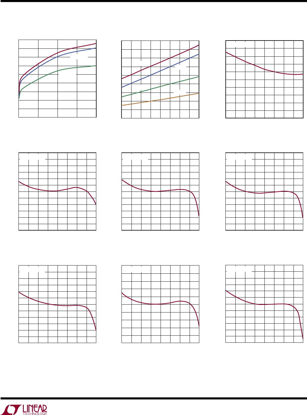
ves in the Typical
Performance Characteristics section.
Note 8: The SHDN pin can be driven below GND only when tied to the IN
pin directly or through a pull-up resistor. If the SHDN pin is driven below
GND by more than –0.3V while IN is powered, the output will turn on.
Note 9: Output noise is listed for the adjustable version with the ADJ pin
connected to the OUT pin. See the RMS Output Noise vs Load Current
curve in the Typical Performance Characteristics Section.
ELECTRICAL CHARACTERISTICS
The l denotes the specifications which apply over the full operating
temperature range, otherwise specifications are at T
J
= 25°C. (Note 2)