LT3007 Series
9
3007fa
For more information www.linear.com/LT3007
PIN FUNCTIONS
SHDN (Pin 1): Shutdown. Pulling the SHDN pin low puts
the LT3007 into a low power state and turns the output
off. If unused, tie the SHDN pin to V
IN
. The LT3007 does
not function if the SHDN pin is not connected. The SHDN
pin cannot be driven below GND unless tied to the IN pin.
If the SHDN pin is driven below GND while IN is powered,
the output will turn on. SHDN pin logic cannot be refer
-
enced to a negative rail.
GND
(
Pins 2, 3, 4): Ground. Connect the bottom of the
resistor divider that sets output voltage directly to GND
for the best regulation.
IN (Pin 5): Input. The IN pin supplies power to the device.
The LT3007 requires a bypass capacitor at IN if the device
is more than six inches away from the main input filter
capacitor. In general, the output impedance of a battery
rises with frequency, so it is advisable to include a bypass
capacitor in battery-powered circuits. A bypass capacitor
in the range of 0.1µF to 10µF will suffice. The LT3007
withstands reverse voltages on the IN pin with respect to
ground and the OUT pin. In the case
of a reversed input,
which occurs with a battery plugged in backwards, the
LT3007 acts as if a blocking diode is in series with its
input. No reverse current flows into the LT3007 and no
reverse voltage appears at the load. The device protects
both itself and the load.
NC (Pin 6): No Connect. Pin 6 is an NC pin in the TSOT-23
package. This pin is not tied to any internal circuitry. LTC
recommends that the NC pin be floated for fault tolerant
operation.
OUT (Pin 7): Output. This pin supplies power to the load.
Use a minimum output capacitor of 2.2µF to prevent os
-
cillations. Large load transient applications require larger
output capacitors to limit peak voltage transients. See the
Applications Information section for more information on
output capacitance and reverse-output characteristics.
ADJ (Pin 8): Adjust. This pin is the error amplifier’s inverting
terminal. Its 400pA typical input bias current flows out of
the pin (see curve of ADJ Pin Bias Current vs Temperature
in the Typical Performance Characteristics section). The
ADJ pin voltage is 600mV referenced to GND and the
output voltage range is 600mV to 44.5V.
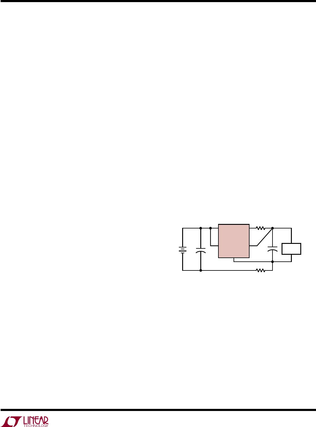
SENSE (Pin 8): Sense. For fixed voltage versions of the
LT3007
(LT3007-1.2, LT3007-1.5, LT3007-1.8, LT3007-
2.5, LT3007-3.3, LT3007-5), the SENSE pin is the input to
the error amplifier. Optimum regulation is obtained at the
point where the SENSE pin is connected to the OUT pin of
the regulator. In critical applications, small voltage drops
are caused by the resistance (RP) of PC traces between
the regulator and the load. These may be eliminated by
connecting the SENSE pin to the output at the load as
shown in Figure 1 (Kelvin Sense Connection). Note that
the voltage drop across the external PC traces add to the
dropout voltage of the regulator. The SENSE pin bias current
is 1µA at the nominal rated output voltage. The SENSE pin
can be pulled below ground (as in a dual supply system
where the regulator load is returned to a negative supply)
and still allow the device to start and operate.
Figure 1. Kelvin Sense Connection
IN
SHDN
3007 F01
R
P
OUT
V
IN
SENSE
GND
LT3007
R
P
+
+
LOAD