IDT5V49EE503
EEPROM PROGRAMMABLE CLOCK GENERATOR CLOCK SYNTHESIZER
IDT®
EEPROM PROGRAMMABLE CLOCK GENERATOR 19
IDT5V49EE503 REV Q 071015
AC Timing Electrical Characteristics
(Spread Spectrum Generation = OFF)
Symbol Parameter Test Conditions Min. Typ. Max. Units
f
IN
1
1.Practical lower frequency is determined by loop filter settings.
Input Frequency
Input frequency limit (CLKIN) 1 200 MHz
Input frequency limit (XIN/REF) 8 100 MHz
1 / t1 Output Frequency 0.001 200 MHz
f
VCO
VCO Frequency VCO operating frequency range 100 1200 MHz
f
PFD
PFD Frequency PFD operating frequency range 0.5
1
100 MHz
f
BW
Loop Bandwidth Based on loop filter resistor and capacitor
values
0.01 10 MHz
t2 Input Duty Cycle Duty Cycle for input 40 60 %
t3 Output Duty Cycle Measured at V
DD
/2, all outputs except
Reference output
45 55 %
Measured at V
DD
/2, Reference output 40 60 %
t4
2
2.A slew rate of 2.75V/ns or greater should be selected for output frequencies of 100MHz or higher.
Slew Rate, SLEW[1:0] = 00 Single-ended 3.3V LVCMOS output clock rise
and fall time, 20% to 80% of V
DD
(Output Load = 5 pF)
3.5 V/ns
Slew Rate, SLEW[1:0] = 01 Single-ended 3.3V LVCMOS output clock rise
and fall time, 20% to 80% of V
DD
(Output Load = 5 pF)
2.75
Slew Rate, SLEW[1:0] = 10 Single-ended 3.3V LVCMOS output clock rise
and fall time, 20% to 80% of V
DD
(Output Load = 5 pF)
2
Slew Rate, SLEW[1:0] = 11 Single-ended 3.3V LVCMOS output clock rise
and fall time, 20% to 80% of V
DD
(Output Load = 5 pF)
1.25
t5 Clock Jitter
6
Peak-to-peak period jitter, 1PLL, multiple
output frequencies switching
80 100 ps
Peak-to-peak period jitter, all 4 PLLs on
3
3.Jitter measured with clock outputs of 27 MHz, 48 MHz, 24.576 MHz, 74.25 MHz and 25 MHz.
200 270 ps
t6 Output Skew Skew between output to output on the same
bank
75 ps
t7
4
4.Includes loading the configuration bits from EEPROM to PLL registers. It does not include EEPROM programming/write time.
Lock Time PLL lock time from power-up 10 20 ms
t8
5
5.Actual PLL lock time depends on the loop configuration.
6. Not guaranteed until customer specific configuration is approved by IDT.
Lock Time PLL lock time from shutdown mode 2 ms
IDT5V49EE503
EEPROM PROGRAMMABLE CLOCK GENERATOR CLOCK SYNTHESIZER
IDT®
EEPROM PROGRAMMABLE CLOCK GENERATOR 20
IDT5V49EE503 REV Q 071015
Spread Spectrum Generation Specifications
Test Circuits and Conditions
Test Circuits for DC Outputs
Symbol Parameter Description Min Typ Max Unit
f
IN
1
1.Practical lower frequency is determined by loop filter settings.
2. Not guaranteed until customer specific configuration is approved by IDT.
Input Frequency Input Frequency Limit 1 400 MHz
f
MOD
Mod Frequency Modulation Frequency 33 120 kHz
f
SPREAD
2
Spread Value Amount of Spread Value (programmable) - Down Spread -0.5 -4.0 %f
OUT
Amount of Spread Value (programmable) - Center Spread ±0.25 ±2.0
OUTx
V
DD
CLK
OUT
GND
C
L
=5pF
0.1µF
V
DDOx
0.1µF
IDT5V49EE503
EEPROM PROGRAMMABLE CLOCK GENERATOR CLOCK SYNTHESIZER
IDT®
EEPROM PROGRAMMABLE CLOCK GENERATOR 21
IDT5V49EE503 REV Q 071015
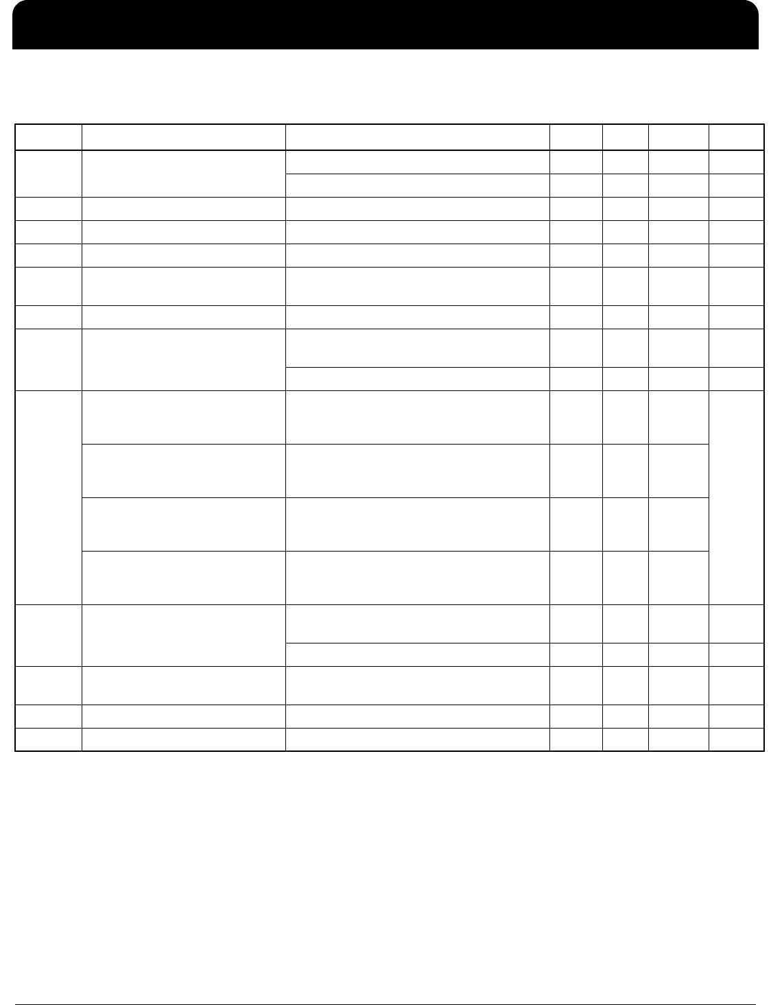
Programming Registers Table
Addr
Default
Register
Hex
Value
Bit #
Description
7654321 0
0x00 00
Reserved HW/SW
Hardware/Software Mode control
HW/SW - 0=HW, 1=SW
0x01 00
Reserved SEL[2:0]
SEL[2:0] - selects configuration in
SW mode
0x02 02
SP OE6 Reserved Reserved OE3 OE2 OE1 OE0
OEx=Output Power Suspend
function for OUTx (‘1’=OUTx will
be suspended on SD/OE pin.
Disable mode is defined by OEMx
bits), ‘0’=outputs enabled and no
association with OE pin (default).
0x03 02
Reserved OS*6 Reserved Reserved OS*3 OS*2 OS*1 OS*0
OS*[6:0] - output suspend, active
low. Overwrites OE setting.
0x04 0F
SH OS*Reserved PLLS*[3:0]
PLLS*[3:0] - PLL Suspend, active
low
SH - shutdown/OE configuration
0x05 04
Reserved XTCLKSEL Reserved
XTCLKSEL - crystal/clock select.
0=Crytal, 1=ICLK
0x06 00
Reserved
0x07 00
Reserved
XTAL[4:0] XTAL[4:0] - crystal cap
0x08 00
Reserved
0x09 00
Reserved
0x0A 10
CZ0_CFG4 IP0[2:0]_CFG4 RZ0[3:0]_CFG4
PLL0 loop parameter
0x0B 10
CZ0_CFG5 IP0[2:0]_CFG5 RZ0[3:0]_CFG5
0x0C 10
CZ0_CFG0 IP0[2:0]_CFG0 RZ0[3:0]_CFG0
0x0D 10
CZ0_CFG1 IP0[2:0]_CFG1 RZ0[3:0]_CFG1
0x0E 10
CZ0_CFG2 IP0[2:0]_CFG2 RZ0[3:0]_CFG2
0x0F 10
CZ0_CFG3 IP0[2:0]_CFG3 RZ0[3:0]_CFG3
0x10 00
Reserved D0[6:0]_CFG0
PLL0 input divider and input sel
D0[6:0] - 127 step Ref Div
D0 = 0 means power down.
0x11 00
Reserved D0[6:0]_CFG1
0x12 00
Reserved D0[6:0]_CFG2
0x13 00
Reserved D0[6:0]_CFG3
0x14 00
Reserved D0[6:0]_CFG4
0x15 00
Reserved D0[6:0]_CFG5
0x16 01
N0[7:0]_CFG4
N - Feedback Divider
2 - 4095 (values of “0” and “1” are
not allowed) Total feedback with
A, using provided calculation
0x17 01
N0[7:0]_CFG5
0x18 01
N0[7:0]_CFG0
0x19 01
N0[7:0]_CFG1
0x1A 01
N0[7:0]_CFG2
0x1B 01
N0[7:0]_CFG3
0x1C 00
A0[3:0]_CFG0 N0[11:8]_CFG0
0x1D 00
A0[3:0]_CFG1 N0[11:8]_CFG1
0x1E 00
A0[3:0]_CFG2 N0[11:8]_CFG2
0x1F 00
A0[3:0]_CFG3 N0[11:8]_CFG3
0x20 00
A0[3:0]_CFG4 N0[11:8]_CFG4
0x21 00
A0[3:0]_CFG5 N0[11:8]_CFG5
0x22 10
CZ1_CFG4 IP1[2:0]_CFG4 RZ1[3:0]_CFG4
PLL1 Loop Parameter
0x23 10
CZ1_CFG5 IP1[2:0]_CFG5 RZ1[3:0]_CFG5
0x24 10
CZ1_CFG0 IP1[2:0]_CFG0 RZ1[3:0]_CFG0
0x25 10
CZ1_CFG1 IP1[2:0]_CFG1 RZ1[3:0]_CFG1
0x26 10
CZ1_CFG2 IP1[2:0]_CFG2 RZ1[3:0]_CFG2
0x27 10
CZ1_CFG3 IP1[2:0]_CFG3 RZ1[3:0]_CFG3

5V49EE503NLGI

Mfr. #:
Manufacturer:
IDT
Description:
Clock Generators & Support Products EEPROM PROGRAMMABLE PLL
Lifecycle:
New from this manufacturer.
Delivery:
DHL FedEx Ups TNT EMS
Payment:
T/T Paypal Visa MoneyGram Western Union

Products related to this Datasheet