16
LTC1292/LTC1297
12927fb
Figure 12. “+” and “–” Input Settling Windows for the LTC1297
“–” input voltage be free of noise and settle completely
during the first CLK cycle of the conversion. Minimizing
R
SOURCE
– and C2 will improve settling time. If large “–”
input source resistance must be used the time can be
extended by using a slower CLK frequency. At the maximum
CLK frequency of 1MHz, R
SOURCE
– < 250
and C2 < 20pF
will provide adequate settling.
Input Op Amps
When driving the analog inputs with an op amp it is
important that the op amp settles within the allowed time
(see Figures 11a, 11b, 11c and 12). Again the “+” and “–
” input sampling times can be extended as described
above to accommodate slower op amps. Most op amps
including the LT1797 and LT1677 single supply op amps
can be made to settle well even with the minimum settling
windows of 3.0µs for the LTC1292 or 6.0µs for the
LTC1297 (“+” input) and 1µs (“–” input) that occurs at the
maximum clock rate of 1MHz. Figures 13 and 14 show
examples of both adequate and poor op amp settling.
VERTICAL: 5mV/DIV
HORIZONTAL: 500ns/DIV
HORIZONTAL: 20µs/DIV
Figure 13. Adequate Settling of Op Amp Driving Analog Input
VERTICAL: 5mV/DIV
Figure 14. Poor Op Amp Settling Can Cause A/D Errors
U
S
A
O
PP
L
IC
AT
I
WU
U
I FOR ATIO
D
OUT
CLK
B11
HI-Z
B10
LTC1292/7 F12
CS
1ST BIT TEST (–) INPUT MUST
SETTLE DURING THIS TIME
t
WHCS
t
SMPL
(+) INPUT MUST SETTLE
DURING THIS TIME
(+) INPUT
(–) INPUT
t
suCS
17
LTC1292/LTC1297
12927fb
RC Input Filtering
It is possible to filter the inputs with an RC network as
shown in Figure 15. For large values of C
F
(e.g., 1µF) the
capacitive input switching currents are averaged into a net
DC current. A filter should be chosen with a small resistor
and large capacitor to prevent DC drops across the resistor.
The magnitude of the DC current is approximately I
DC
=
100pF × V
IN
/t
CYC
and is roughly proportional to V
IN
. When
running the LTC1292(LTC1297) at the minimum cycle
time of 16.5µs (20µs), the input current equals 30µA
(25µA) at V
IN
= 5V. Here a filter resistor of 4 (5) will
cause 0.1LSB of full scale error. If a large filter resistor
must be used, errors can be reduced by increasing the
cycle time as shown in the typical performance
characteristics curve Maximum Filter Resistor vs Cycle
Time.
Figure 15. RC Input Filtering
curve of S&H Acquisition Time vs Source Resistance). The
input voltage is sampled during the t
SMPL
time as shown
in Figure 11. The sampling interval begins at the rising
edge of CS for the LTC1292, and at the falling edge of CS
for the LTC1297, and continues until the falling edge of the
CLK before the conversion begins. On this falling edge the
S&H goes into the hold mode and the conversion begins.
Differential Input
With a differential input the A/D no longer converts a single
voltage but converts the difference between two voltages.
The voltage on the +IN pin is sampled and held and can be
rapidly time-varying as in single-ended mode. The voltage
on the –IN pin must remain constant and be free of noise
and ripple throughout the conversion time. Otherwise the
differencing operation will not be done accurately. The
conversion time is 12 CLK cycles. Therefore a change in
the –IN input voltage during this interval can cause
conversion errors. For a sinusoidal voltage on the –IN
input this error would be:
VfV
f
ERROR MAX IN PEAK
CLK
( ) (– )
=
()
2
12
π
Where f
(–IN)
is the frequency of the –IN input voltage,
V
PEAK
is its peak amplitude and f
CLK
is the frequency of the
CLK. Usually V
ERROR
will not be significant. For a 60Hz
signal on the –IN input to generate a 0.25LSB error
(300µV) with the converter running at CLK = 1MHz, its
peak value would have to be 66mV. Rearranging the above
equation the maximum sinusoidal signal that can be
digitized to a given accuracy is given as:
f
V
V
f
IN MAX
ERROR MAX
PEAK
CLK
(– )
()
=
π
2
12
For 0.25LSB error (300µV) the maximum input sinusoid
with a 5V peak amplitude that can be digitized is 0.8Hz.
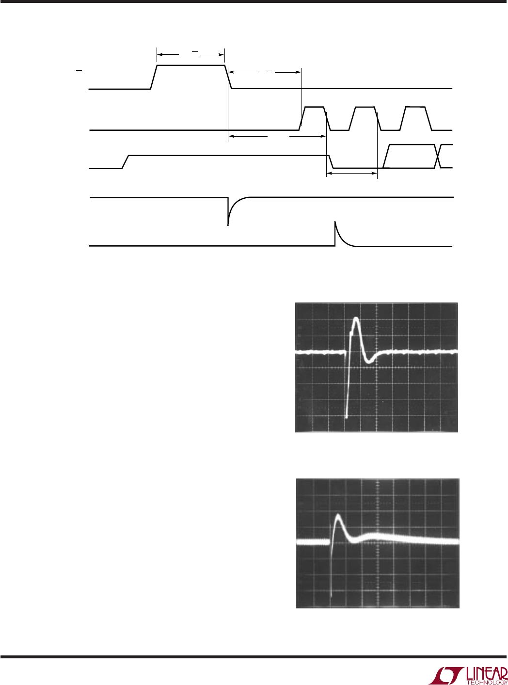
Reference Input
The voltage on the reference input of the LTC1292/
LTC1297 determine the voltage span of the A/D con-
verter. The reference input has transient capacitive
Input Leakage Current
Input leakage currents also can create errors if the source
resistance gets too large. For example, the maximum input
leakage specification of 1µA flowing through a source
resistance of 1k will cause a voltage drop of 1mV or
0.8LSB. This error will be much reduced at lower
temperatures because leakage drops rapidly (see typical
performance characteristics curve Input Channel Leakage
Current vs Temperature).
SAMPLE-AND-HOLD
Single-Ended Input
The LTC1292/LTC1297 provide a built-in sample-and-
hold (S&H) function on the +IN input for signals acquired
in the single-ended mode (–IN pin grounded). The sample-
and-hold allows the LTC1292/LTC1297 to convert rapidly
varying signals (see typical performance characteristics
R
FILTER
C
FILTER
LTC1292/7 F15
LTC1292
LTC1297
“+”
“–”
I
DC
V
IN
U
S
A
O
PP
L
IC
AT
I
WU
U
I FOR ATIO
18
LTC1292/LTC1297
12927fb
U
S
A
O
PP
L
IC
AT
I
WU
U
I FOR ATIO
Figures 17 and 18 show examples of both adequate and
poor settling. Using a slower CLK will allow more time
for the reference to settle. Even at the maximum CLK
rate of 1MHz most references and op amps can be
made to settle within the 1µs bit time. For example the
LT1790 will settle adequately.
Reduced Reference Operation
The effective resolution of the LTC1292/LTC1297 can
be increased by reducing the input span of the con-
verter. The LTC1292/LTC1297 exhibit good linearity
over a range of reference voltages (see typical perfor-
mance characteristics curves of Change in Linearity vs
Reference Voltage). Care must be taken when operat-
ing at low values of V
REF
because of the reduced LSB
step size and the resulting higher accuracy requirement
placed on the converter. Offset and noise are factors
that must be considered when operating at low V
REF
values. The internal reference for V
REF
has been tied to
the GND pin. Any voltage drop from the GND pin to the
ground plane will cause a gain error.
Offset with Reduced V
REF
The offset of the LTC1292/LTC1297 has a larger effect
on the output code when the A/D is operated with a
reduced reference voltage. The offset (which is typi-
cally a fixed voltage) becomes a larger fraction of an
LSB as the size of the LSB is reduced. The typical
performance characteristics curve of Unadjusted Off-
set Error vs Reference Voltage shows how offset in
LSBs is related to reference voltage for a typical value
of V
OS
. For example a V
OS
of 0.1mV, which is 0.1LSB
with a 5V reference becomes 0.4LSB with a 1.25V
reference. If this offset is unacceptable, it can be
corrected digitally by the receiving system or by offset-
ting the –IN input to the LTC1292/LTC1297.
Noise with Reduced V
REF
The total input referred noise of the LTC1292/LTC1297
can be reduced to approximately 200µV
P-P
using a
ground plane, good bypassing, good layout techniques
and minimizing noise on the reference inputs. This
noise is insignificant with a 5V reference input but will
become a larger fraction of an LSB as the size of the LSB
switching currents due to the switched-capacitor con-
version technique (see Figure 16). During each bit test
of the conversion (every CLK cycle) a capacitive current
spike will be generated on the reference pin by the A/D.
These current spikes settle quickly and do not cause a
problem. If slow settling circuitry is used to drive the
reference input, take care to insure that transients
caused by these current spikes settle completely during
each bit test of the conversion.
R
ON
8pF TO 40pF
LTC1292
LTC1297
REF
+
R
OUT
V
REF
EVERY
CLK CYCLE
14
13
REF
LTC1292/7 F16
Figure 16. Reference Input Equivalent Circuit
HORIZONTAL: 1µs/DIV
Figure 17. Adequate Reference Settling (LT1027)
HORIZONTAL: 10µs/DIV
Figure 18. Poor Reference Settling Can Cause A/D Errors
VERTICAL: 0.5mV/DIV
VERTICAL: 0.5mV/DIV

LTC1292CIN8#PBF

Mfr. #:
Manufacturer:
Analog Devices Inc.
Description:
Analog to Digital Converters - ADC 12-Bit Serial I/O Diff Input ADC
Lifecycle:
New from this manufacturer.
Delivery:
DHL FedEx Ups TNT EMS
Payment:
T/T Paypal Visa MoneyGram Western Union