4
LTC1292/LTC1297
12927fb
LTC1292B/LTC1297B
LTC1292C/LTC1297C
LTC1292D/LTC1297D
SYMBOL PARAMETER CONDITIONS MIN TYP MAX UNITS
I
CC
Positive Supply Current CS High LTC1292 ● 612 mA
CS Low LTC1297 ● 612 mA
CS High Power Shutdown CLK Off LTC1297 ● 510 µA
I
REF
Reference Current CS High ● 10 50 µA
DIGITAL A D DC ELECTRICAL CHARACTERISTICS
U
CCHARA TERIST
ICS
UW
AT
Y
P
I
CA
LPER
F
O
R
C
E
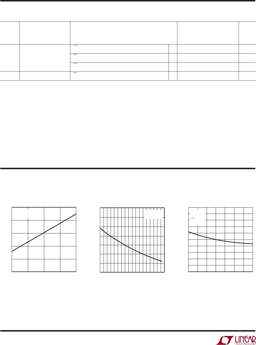
AMBIENT TEMPERATURE (°C)
–50
SUPPLY CURRENT (mA)
7
8
9
30 70
LTC1292/7 G02
6
5
–30 –10
50 90
110
4
3
10
10
130
CLK = 1MHz
V
CC
= 5V
SUPPLY VOLTAGE (V)
4
SUPPLY CURRENT (mA)
4
6
6
LTC1292/7 G01
2
0
5
10
8
CLK = 1MHz
T
A
= 25°C
LTC1297 Supply Current (Power
Shutdown) vs Temperature
AMBIENT TEMPERATURE (°C)
–50
0
SUPPLY CURRENT (µA)
1
3
4
5
10
7
0
50
75
LTC1292/7 G03
2
8
9
6
–25
25
100
125
V
CC
= 5V
V
REF
= 5V
CS HIGH
CLK OFF
Supply Current vs TemperatureSupply Current vs Supply Voltage
below GND or one diode drop above V
CC
. Be careful during testing at low
V
CC
levels (4.5V), as high level reference or analog inputs (5V) can cause
this input diode to conduct, especially at elevated temperatures, and cause
errors for inputs near full scale. This spec allows 50mV forward bias of
either diode. This means that as long as the reference or analog input does
not exceed the supply voltage by more than 50mV, the output code will be
correct. To achieve an absolute 0V to 5V input voltage range will therefore
require a minimum supply voltage of 4.950V over initial tolerance,
temperature variations and loading.
Note 8: Channel leakage current is measured after the channel selection.
Note 9: Increased leakage currents at elevated temperatures cause the
S/H to droop, therefore it is recommended that f
CLK
≥125kHz at 125°C,
f
CLK
≥ 31kHz at 85°C, and f
CLK
≥ 3kHz at 25°C.
Note 1: Absolute Maximum Ratings are those values beyond which the life
of a device may be impaired.
Note 2: All voltage values are with respect to ground (unless otherwise
noted).
Note 3: V
CC
= 5V, V
REF
= 5V, CLK = 1.0MHz unless otherwise specified.
Note 4: One LSB is equal to V
REF
divided by 4096. For example, when
V
REF
= 5V, 1LSB = 5V/4096 = 1.22mV.
Note 5: Linearity error is specified between the actual end points of the
A/D transfer curve. The deviation is measured from the center of the
quantization band.
Note 6: Recommended operating conditions.
Note 7: Two on-chip diodes are tied to each reference and analog input
which will conduct for reference or analog input voltages one diode drop
The ● denotes the specifications which
apply over the full operating temperature range, otherwise specifications are at T
A
= 25°C. (Note 3)