8
LTC1292/LTC1297
12927fb
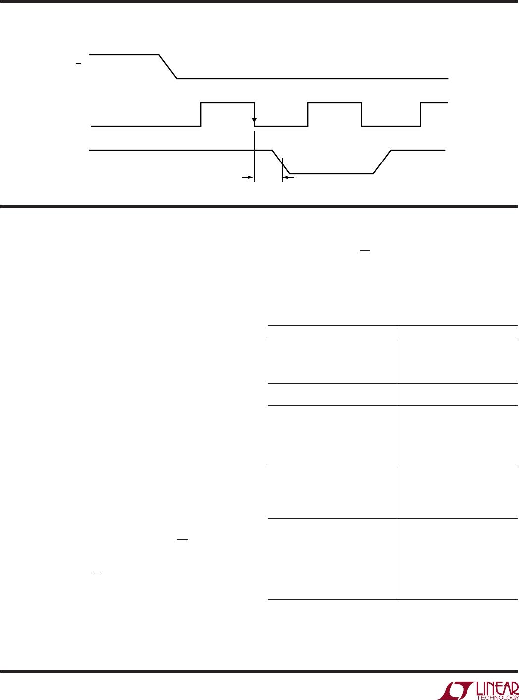
TEST CIRCUITS
Voltage Waveforms for t
en
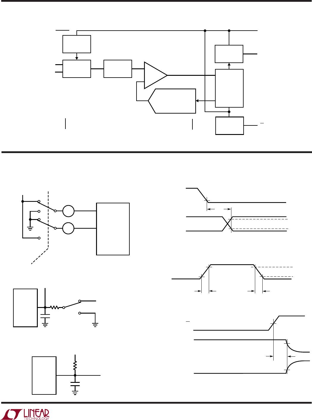
The LTC1292/LTC1297 are data acquisition components
which contain the following functional blocks:
1. 12-Bit Succesive Approximation Capacitive A/D
Converter
2. Differential Input
3. Sample-and-Hold (S/H)
4. Synchronous, Half-Duplex Serial Interface
5. Control and Timing Logic
DIGITAL CONSIDERATIONS
Serial Interface
The LTC1292/LTC1297 communicate with microproces-
sors and other external circuitry via a synchronous, half-
duplex, three-wire serial interface (see Operating Se-
quence). The clock (CLK) synchronizes the data transfer
with each bit being transmitted on the falling CLK edge.
The LTC1292/LTC1297 do not require a configuration
input word and have no D
IN
pin. They are permanently
configured to have a single differential input and to per-
form a unipolar conversion. A falling CS initiates data
transfer. To allow the LTC1297 to recover from the power
shutdown mode, t
suCS
has to be met. Then the first CLK
pulse enables D
OUT
. After one null bit, the A/D conversion
result is output on the D
OUT
line with a MSB-first sequence
followed by a LSB-first sequence. With the half-duplex
serial interface the D
OUT
data is from the current conver-
sion. This provides easy interface to MSB-first or LSB-first
U
S
A
O
PP
L
IC
AT
I
WU
U
I FOR ATIO
serial ports. Bringing CS high resets the LTC1292/LTC1297
for the next data exchange and puts the LTC1297 into its
power shutdown mode.
Table 1. Microprocessor with Hardware Serial Interfaces
Compatible with the LTC1292/LTC1297**
D
OUT
0.8V
t
en
B11
CS
CLK
LTC1292/7 TC07
PART NUMBER TYPE OF INTERFACE
Motorola
MC6805S2, S3 SPI
MC68HC11 SPI
MC68HC05 SPI
RCA
CDP68HC05 SPI
Hitachi
HD6305 SCI Synchronous
HD6301 SCI Synchronous
HD63701 SCI Synchronous
HD6303 SCI Synchronous
HD64180 SCI Synchronous
National Semiconductor
COP400 Family MICROWIRE
†
COP800 Family MCROWIRE/PLUS
†
NS8050U MICROWIRE/PLUS
HPC16000 Family MICROWIRE/PLUS
Texas Instruments
TMS7002 Serial Port
TMS7042 Serial Port
TMS70C02 Serial Port
TMS70C42 Serial Port
TMS32011* Serial Port
TMS32020* Serial Port
TMS370C050 SPI
* Requires external hardware
** Contact factory for interface information for processors not on this list
†
MICROWIRE and MICROWIRE/PLUS are trademarks of National
Semiconductor Corp.