LTC1992 Family
1
1992fb
TYPICAL APPLICATION
FEATURES DESCRIPTION
Low Power, Fully Differential
Input/Output
Amplifier/Driver Family
The LTC
®
1992 product family consists of five fully differen-
tial, low power amplifiers. The LTC1992 is an unconstrained
fully differential amplifier. The LTC1992-1, LTC1992-2,
LTC1992-5 and LTC1992-10 are fixed gain blocks (with
gains of 1, 2, 5 and 10 respectively) featuring precision
on-chip resistors for accurate and ultrastable gain. All of
the LTC1992 parts have a separate internal common mode
feedback path for outstanding output phase balancing
and reduced second order harmonics. The V
OCM
pin sets
the output common mode level independent of the input
common mode level. This feature makes level shifting of
signals easy.
The amplifiers’ differential inputs operate with signals
ranging from rail-to-rail with a common mode level from
the negative supply up to 1.3V from the positive supply.
The differential input DC offset is typically 250μV. The
rail-to-rail outputs sink and source 10mA. The LTC1992
is stable for all capacitive loads up to 10,000pF.
The LTC1992 can be used in single supply applications
with supply voltages as low as 2.7V. It can also be used
with dual supplies up to ±5V. The LTC1992 is available in
an 8-pin MSOP package.
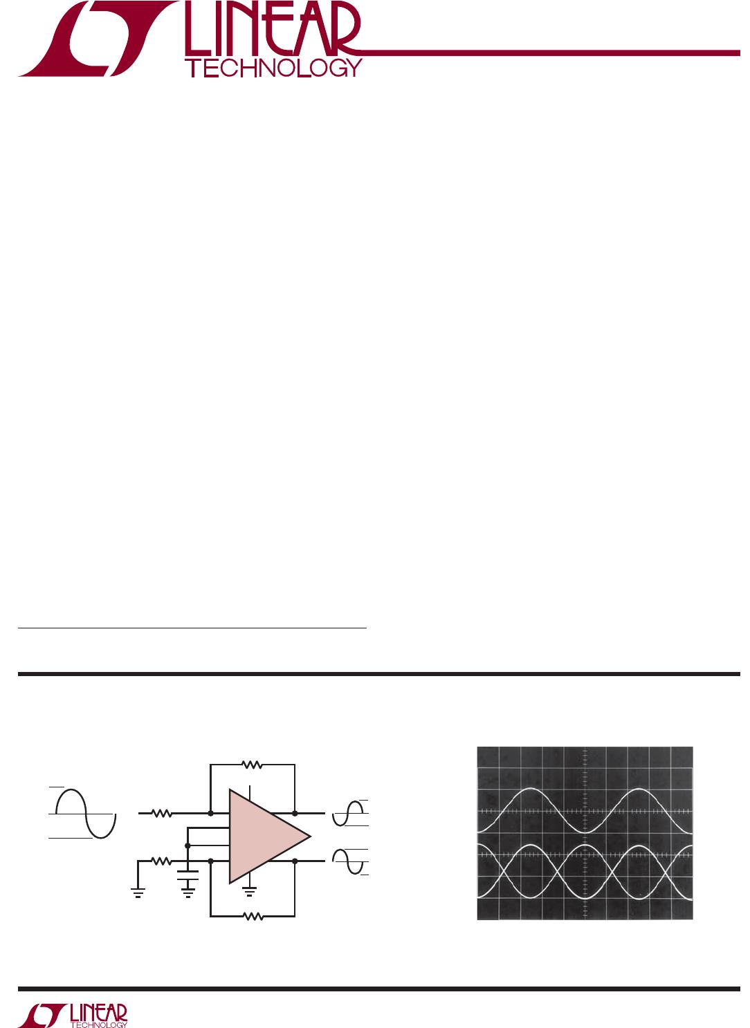
Single-Supply, Single-Ended to Differential Conversion
APPLICATIONS
n
Available with Adjustable Gain or Fixed Gain of 1,
2, 5 or 10
n
±0.3% (Max) Gain Error from –40°C to 85°C
n
3.5ppm/°C Gain Temperature Coefficient
n
5ppm Gain Long Term Stability
n
Fully Differential Input and Output
n
C
LOAD
Stable up to 10,000pF
n
Adjustable Output Common Mode Voltage
n
Rail-to-Rail Output Swing
n
Low Supply Current: 1mA (Max)
n
High Output Current: 10mA (Min)
n
Specified on a Single 2.7V to ±5V Supply
n
DC Offset Voltage <2.5mV (Max)
n
Available in 8-Lead MSOP Package
n
Differential Driver/Receiver
n
Differential Amplification
n
Single-Ended to Differential Conversion
n
Level Shifting
n
Trimmed Phase Response for Multichannel Systems
L, LT, LTC, LTM, Linear Technology and the Linear logo are registered trademarks of Linear
Technology Corporation. All other trademarks are the property of their respective owners.
+
+
5V
5V
LTC1992
3
6
V
OCM
V
MID
0V
2.5V
0V
V
IN
0.01μF
1992 TA01a
4
5
2
7
8
1
10k
10k
10k
10k
5V
0V
5V
–5V
2.5V
INPUT SIGNAL
FROM A
±5V SYSTEM
OUTPUT SIGNAL
FROM A
SINGLE-SUPPLY SYSTEM
V
IN
(5V/DIV)
+OUT
–OUT
(2V/DIV)
5V
0V
–5V
5V
0V
1992 TA01b
LTC1992 Family
2
1992fb
ABSOLUTE MAXIMUM RATINGS
Total Supply Voltage (+V
S
to –V
S
) ............................. 12V
Maximum Voltage
on any Pin ................ (–V
S
– 0.3V) ≤ V
PIN
≤ (+V
S
+ 0.3V)
Output Short-Circuit Duration (Note 3) ............ Indefinite
Operating Temperature Range (Note 5)
LTC1992CMS8/LTC1992-XCMS8/
LTC1992IMS8/LTC1992-XIMS8 ...........40°C to 85°C
LTC1992HMS8/LTC1992-XHMS8 ...... 40°C to 125°C
(Note 1)
PIN CONFIGURATION
ORDER INFORMATION
LEAD FREE FINISH TAPE AND REEL PART MARKING* PACKAGE DESCRIPTION SPECIFIED TEMPERATURE RANGE
LTC1992CMS8#PBF LTC1992CMS8#TRPBF LTYU 8-Lead Plastic MSOP 0°C to 70°C
LTC1992IMS8#PBF LTC1992IMS8#TRPBF LTYU 8-Lead Plastic MSOP –40°C to 85°C
LTC1992HMS8#PBF LTC1992HMS8#TRPBF LTYU 8-Lead Plastic MSOP –40°C to 125°C
LTC1992-1CMS8#PBF LTC1992-1CMS8#TRPBF LTACJ 8-Lead Plastic MSOP 0°C to 70°C
LTC1992-1IMS8#PBF LTC1992-1IMS8#TRPBF LTACJ 8-Lead Plastic MSOP –40°C to 85°C
LTC1992-1HMS8#PBF LTC1992-1HMS8#TRPBF LTACJ 8-Lead Plastic MSOP –40°C to 125°C
LTC1992-2CMS8#PBF LTC1992-2CMS8#TRPBF LTYV 8-Lead Plastic MSOP 0°C to 70°C
LTC1992-2IMS8#PBF LTC1992-2IMS8#TRPBF LTYV 8-Lead Plastic MSOP –40°C to 85°C
LTC1992-2HMS8#PBF LTC1992-2HMS8#TRPBF LTYV 8-Lead Plastic MSOP –40°C to 125°C
LTC1992-5CMS8#PBF LTC1992-5CMS8#TRPBF LTACK 8-Lead Plastic MSOP 0°C to 70°C
LTC1992-5IMS8#PBF LTC1992-5IMS8#TRPBF LTACK 8-Lead Plastic MSOP –40°C to 85°C
LTC1992-5HMS8#PBF LTC1992-5HMS8#TRPBF LTACK 8-Lead Plastic MSOP –40°C to 125°C
LTC1992-10CMS8#PBF LTC1992-10CMS8#TRPBF LTACL 8-Lead Plastic MSOP 0°C to 70°C
LTC1992-10IMS8#PBF LTC1992-10IMS8#TRPBF LTACL 8-Lead Plastic MSOP –40°C to 85°C
LTC1992-10HMS8#PBF LTC1992-10HMS8#TRPBF LTACL 8-Lead Plastic MSOP –40°C to 125°C
Consult LTC Marketing for parts specified with wider operating temperature ranges. *The temperature grade is identified by a label on the shipping container.
Consult LTC Marketing for information on non-standard lead based finish parts.
For more information on lead free part marking, go to: http://www.linear.com/leadfree/
For more information on tape and reel specifications, go to: http://www.linear.com/tapeandreel/
Specified Temperature Range (Note 6)
LTC1992CMS8/LTC1992-XCMS8 ............. 0°C to 70°C
LTC1992IMS8/LTC1992-XIMS8 ...........40°C to 85°C
LTC1992HMS8/LTC1992-XHMS8 ...... 40°C to 125°C
Storage Temperature Range .................65°C to 150°C
Lead Temperature (Soldering, 10 sec) ...................300°C
LTC1992 LTC1992-X
1
2
3
4
–IN
V
OCM
+V
S
+OUT
8
7
6
5
+IN
V
MID
–V
S
–OUT
TOP VIEW
MS8 PACKAGE
8-LEAD PLASTIC MSOP
+
+
T
JMAX
= 150°C, θ
JA
= 250°C/W
1
2
3
4
–IN
V
OCM
+V
S
+OUT
8
7
6
5
+IN
V
MID
–V
S
–OUT
TOP VIEW
MS8 PACKAGE
8-LEAD PLASTIC MSOP
+
+
T
JMAX
= 150°C, θ
JA
= 250°C/W
LTC1992 Family
3
1992fb
ELECTRICAL CHARACTERISTICS
The l denotes the specifications which apply over the full operating
temperature range, otherwise specifications are at T
A
= 25°C. +V
S
= 5V, –V
S
= 0V, V
INCM
= V
OUTCM
= V
OCM
= 2.5V, unless otherwise
noted. V
OCM
is the voltage on the V
OCM
pin. V
OUTCM
is defined as (+V
OUT
+ –V
OUT
)/2. V
INCM
is defined as (+V
IN
+ –V
IN
)/2. V
INDIFF
is
defined as (+V
IN
– –V
IN
). V
OUTDIFF
is defined as (+V
OUT
– –V
OUT
). Specifications applicable to all parts in the LTC1992 family.
SYMBOL PARAMETER CONDITIONS
ALL C AND I GRADE ALL H GRADE
UNITSMIN TYP MAX MIN TYP MAX
V
S
Supply Voltage Range
l
2.7 11 2.7 11 V
I
S
Supply Current V
S
= 2.7V to 5V
V
S
= ±5V
l
l
0.65
0.75
0.7
0.8
1.0
1.2
1.2
1.5
0.65
0.8
0.7
0.9
1.0
1.5
1.2
1.8
mA
mA
mA
mA
V
OSDIFF
Differential Offset Voltage
(Input Referred) (Note 7)
V
S
= 2.7V
V
S
= 5V
V
S
= ±5V
l
l
l
±0.25
±0.25
±0.25
±2.5
±2.5
±2.5
±0.25
±0.25
±0.25
±4
±4
±4
mV
mV
mV
ΔV
OSDIFF
/ΔT Differential Offset Voltage Drift
(Input Referred) (Note 7)
V
S
= 2.7V
V
S
= 5V
V
S
= ±5V
l
l
l
10
10
10
10
10
10
μV/°C
μV/°C
μV/°C
PSRR Power Supply Rejection Ratio
(Input Referred) (Note 7)
V
S
= 2.7V to ±5V
l
75 80 72 80 dB
GCM Common Mode Gain(V
OUTCM
/V
OCM
)
Common Mode Gain Error
Output Balance (ΔV
OUTCM
/(ΔV
OUTDIFF
)V
OUTDIFF
= –2V to +2V
l
l
l
1
±0.1
–85
±0.3
–60
1
±0.1
–85
±0.35
–60
%
dB
V
OSCM
Common Mode Offset Voltage
(V
OUTCM
– V
OCM
)
V
S
= 2.7V
V
S
= 5V
V
S
= ±5V
l
l
l
±0.5
±1
±2
±12
±15
±18
±0.5
±1
±2
±15
±17
±20
mV
mV
mV
ΔV
OSCM
/ΔT Common Mode Offset Voltage Drift V
S
= 2.7V
V
S
= 5V
V
S
= ±5V
l
l
l
10
10
10
10
10
10
μV/°C
μV/°C
μV/°C
V
OUTCMR
Output Signal Common Mode Range
(Voltage Range for the V
OCM
Pin)
l
(–V
S
) + 0.5V (+V
S
) – 1.3V (–V
S
) + 0.5V (+V
S
) – 1.3V V
R
INVOCM
Input Resistance, V
OCM
Pin
l
500 500
I
BVOCM
Input Bias Current, V
OCM
Pin V
S
= 2.7V to ±5V
l
±2 ±2 pA
V
MID
Voltage at the V
MID
Pin
l
2.44 2.50 2.56 2.43 2.50 2.57 V
V
OUT
Output Voltage, High
(Note 2)
V
S
= 2.7V, Load = 10k
V
S
= 2.7V, Load = 5mA
V
S
= 2.7V, Load = 10mA
l
l
l
2.60
2.50
2.29
2.69
2.61
2.52
2.60
2.50
2.29
2.69
2.61
2.52
V
V
V
Output Voltage, Low
(Note 2)
V
S
= 2.7V, Load = 10k
V
S
= 2.7V, Load = 5mA
V
S
= 2.7V, Load = 10mA
l
l
l
0.02
0.10
0.20
0.10
0.25
0.35
0.02
0.10
0.20
0.10
0.25
0.41
V
V
V
Output Voltage, High
(Note 2)
V
S
= 5V, Load = 10k
V
S
= 5V, Load = 5mA
V
S
= 5V, Load = 10mA
l
l
l
4.90
4.85
4.75
4.99
4.90
4.81
4.90
4.80
4.70
4.99
4.90
4.81
V
V
V
Output Voltage, Low
(Note 2)
V
S
= 5V, Load = 10k
V
S
= 5V, Load = 5mA
V
S
= 5V, Load = 10mA
l
l
l
0.02
0.10
0.20
0.10
0.25
0.35
0.02
0.10
0.20
0.10
0.30
0.42
V
V
V
Output Voltage, High
(Note 2)
V
S
= ±5V, Load = 10k
V
S
= ±5V, Load = 5mA
V
S
= ±5V, Load = 10mA
l
l
l
4.90
4.85
4.65
4.99
4.89
4.80
4.85
4.80
4.60
4.99
4.89
4.80
V
V
V
Output Voltage, Low
(Note 2)
V
S
= ±5V, Load = 10k
V
S
= ±5V, Load = 5mA
V
S
= ±5V, Load = 10mA
l
l
l
–4.99
–4.90
–4.80
–4.90
–4.75
–4.65
–4.98
–4.90
–4.80
–4.85
–4.75
–4.55
V
V
V

LTC1992-2HMS8#TRPBF

Mfr. #:
Manufacturer:
Analog Devices Inc.
Description:
Differential Amplifiers L Pwr, Fully Diff In/Out Amp/Drvr Fam
Lifecycle:
New from this manufacturer.
Delivery:
DHL FedEx Ups TNT EMS
Payment:
T/T Paypal Visa MoneyGram Western Union