LTC1992 Family
35
1992fb
APPLICATIONS INFORMATION
Fully Differential Amplifier Applications
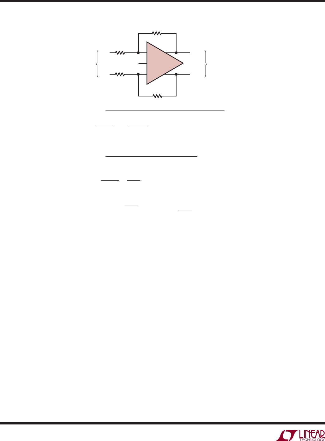
Circuit Analysis
All of the previous applications circuit discussions have as-
sumed perfectly matched symmetrical feedback networks.
To consider the effects of mismatched or asymmetrical
feedback networks, the equations get a bit messier.
Figure 6 lists the basic gain equation for the differential
output voltage in terms of +V
IN
, –V
IN
, V
OSDIFF
, V
OUTCM
and the feedback factors β1 and β2. The feedback factors
are simply the portion of the output that is fed back to the
input summing junction by the R
FB
-R
IN
resistive voltage
divider. β1 and β2 have the range of zero to one. The
V
OUTCM
term also includes its offset voltage, V
OSCM
, and
its gain mismatch term, K
CM
. The K
CM
term is determined
by the matching of the on-chip R
CMP
and R
CMM
resistors
in the common mode level servo (see Figure 2).
While mathematically correct, the basic signal equation
does not immediately yield any intuitive feel for fully
differential amplifier application operation. However, by
nulling out specific terms, some basic observations and
sensitivities come forth. Setting β1 equal to β2, V
OSDIFF
to zero and V
OUTCM
to V
OCM
gives the old gain equation
from Figure 3. The ground referenced, single-ended input
signal equation yields the interesting result that the driven
side feedback factor (β1) has a very different sensitivity
than the grounded side (β2). The CMRR is twice the
feedback factor difference divided by the feedback fac-
tor sum. The differential output offset voltage has two
terms. The first term is determined by the input offset
term, V
OSDIFF
, and the application’s gain. Note that this
term equates to the formula in Figure 3 when β1 equals
β2. The amount of signal level shifting and the feedback
factor mismatch determines the second term. This term
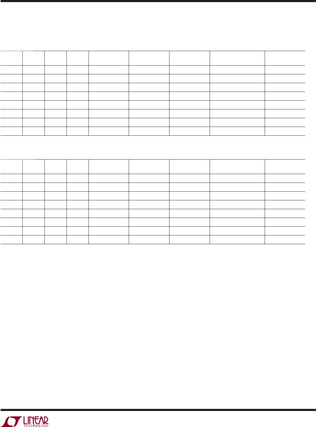
Table 1. Input Signal Limitations for Some Common Applications
Single Supply Ground Referenced Single-Ended Input Signal, V
OCM
at Mid-Supply. (The V
INSIG
Min and Max values listed account for
both the input common mode limits and the output clipping)
Single Supply Ground Referenced Single-Ended Input Signal, V
OCM
at Typical ADC Reference Levels. (The V
INSIG
Min and Max values
listed account for both the input common mode limits and the output clipping)
+V
S
(V)
–V
S
(V)
GAIN
(V/V)
V
OCM
(V)
V
INREF
(V)
V
INSIG(MAX)
(V)
V
INSIG(MIN)
(V)
V
INSIGP-P(MAX)
(V
P-P
AROUND V
INREF
)
V
OUTDIFF(MAX)
(V
P-PDIFF
)
2.7 0 1 1.35 0 2.700 –2.700 5.40 5.40
2.7 0 2 1.35 0 1.350 –1.350 2.70 5.40
2.7 0 5 1.35 0 0.540 –0.540 1.08 5.40
2.7 0 10 1.35 0 0.270 –0.270 0.54 5.40
5 0 1 2.5 0 5.000 –5.000 10.00 10.00
5 0 2 2.5 0 2.500 –2.500 5.00 10.00
5 0 5 2.5 0 1.000 –1.000 2.00 10.00
5 0 10 2.5 0 0.500 –0.500 1.00 10.00
+V
S
(V)
–V
S
(V)
GAIN
(V/V)
V
OCM
(V)
V
INREF
(V)
V
INSIG(MAX)
(V)
V
INSIG(MIN)
(V)
V
INSIGP-P(MAX)
(V
P-P
AROUND V
INREF
)
V
OUTDIFF(MAX)
(V
P-PDIFF
)
2.7 0 1 1 0 2.000 –2.000 4.00 4.00
2.7 0 2 1 0 1.000 –1.000 2.00 4.00
2.7 0 5 1 0 0.400 –0.400 0.80 4.00
2.7 0 10 1 0 0.200 –0.200 0.40 4.00
5 0 1 2 0 4.000 –4.000 8.00 8.00
5 0 2 2 0 2.000 –2.000 4.00 8.00
5 0 5 2 0 0.800 –0.800 1.60 8.00
5 0 10 2 0 0.400 –0.400 0.80 8.00