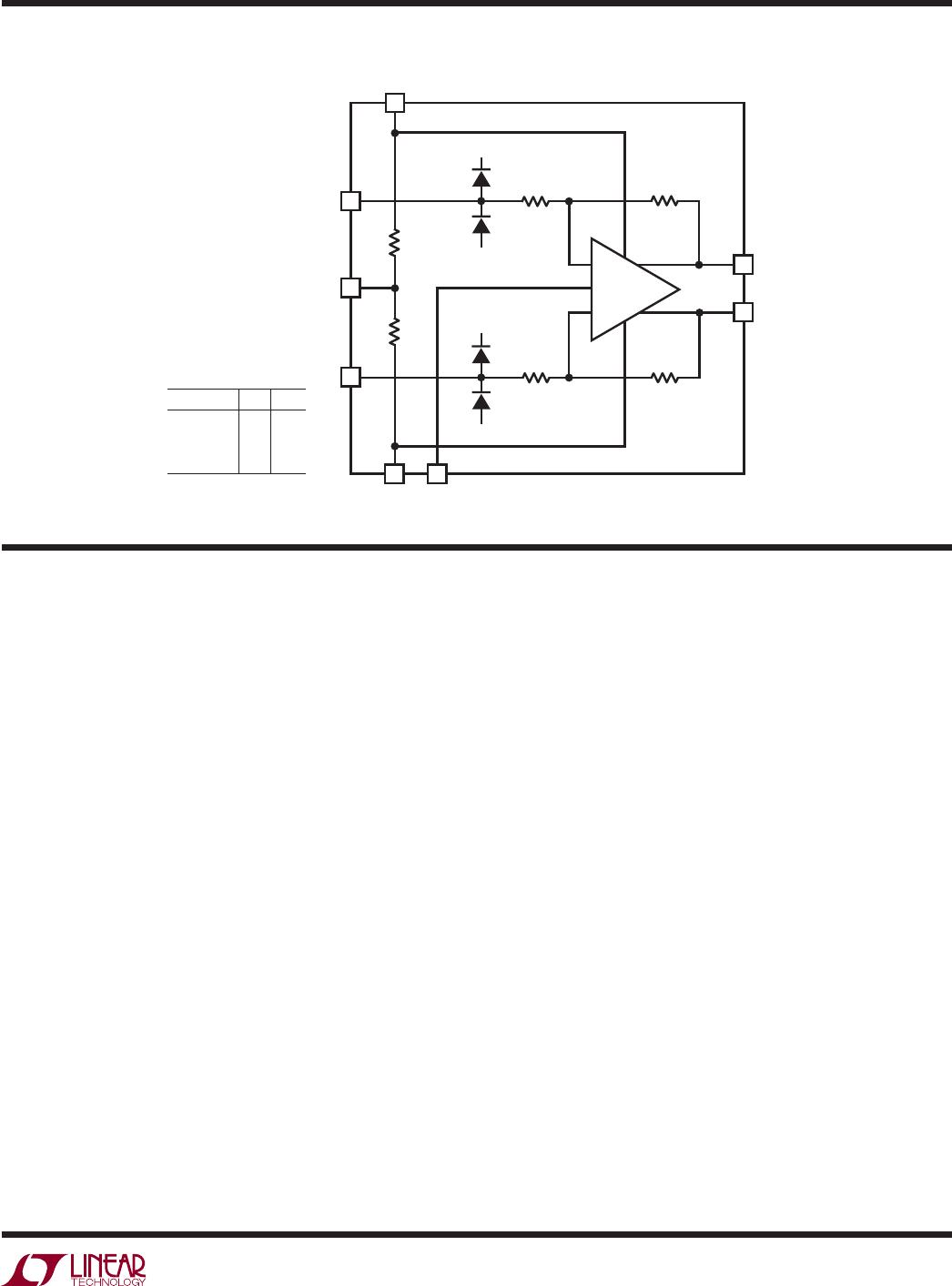
LTC1992 Family
27
1992fb
APPLICATIONS INFORMATION
negative feedback and using an op amp’s differential input
to create the servo’s summing junction.
One servo controls the signal gain path. The differential
input of op amp A1 creates the summing junction of this
servo. Any voltage present at the input of A1 is amplified (by
the op amp’s large open-loop gain), sent to the summing
blocks and then onto the outputs. Taking note of the signs on
the summing blocks, op amp A1’s output moves +OUT and
–OUT in opposite directions. Applying a voltage step at
the INM node increases the +OUT voltage while the –OUT
voltage decreases. The RFB resistors connect the outputs
to the appropriate inputs establishing negative feedback and
closing the servo’s loop. Any servo loop always attempts
to drive its error voltage to zero. In this servo, the error
voltage is the voltage between the INM and INP nodes,
thus A1 will force the voltages on the INP and INM nodes
to be equal (within the part’s DC offset, open loop gain
and bandwidth limits). The “virtual short” between the
two inputs is conceptually the same as that for op amps
and is critical to understanding fully differential amplifier
applications.
The other servo controls the output common mode level.
The differential input of op amp A2 creates the summing
junction of this servo. Similar to the signal gain servo
above, any voltage present at the input of A2 is amplified,
sent to the summing blocks and then onto the outputs.
However, in this case, both outputs move in the same direc-
tion. The resistors R
CMP
and R
CMM
connect the +OUT and
–OUT outputs to A2’s inverting input establishing negative
feedback and closing the servo’s loop. The midpoint of
resistors R
CMP
and R
CMM
derives the output’s common
mode level (i.e., its average). This measure of the output’s
common mode level connects to A2’s inverting input while
A2’s noninverting input connects directly to the V
OCM
pin.
A2 forces the voltages on its inverting and noninverting
inputs to be equal. In other words, it forces the output
common mode voltage to be equal to the voltage on the
V
OCM
input pin.
For any fully differential amplifier application to function
properly both the signal gain servo and the common mode
level servo must be satisfied. When analyzing an applica-
tions circuit, the INP node voltage must equal the INM node
voltage and the output common mode voltage must equal
the V
OCM
voltage. If either of these servos is taken out of
the specified areas of operation (e.g., inputs taken beyond
the common mode range specifications, outputs hitting the
supply rails or input signals varying faster than the part
can track), the circuit will not function properly.
Fully Differential Amplifier Signal Conventions
Fully differential amplifiers have a multitude of signals and
signal ranges to consider. To maintain proper operation
with conventional op amps, the op amp’s inputs and its
output must not hit the supply rails and the input signal’s
common mode level must also be within the part’s speci-
fied limits. These considerations also apply to fully dif-
ferential amplifiers, but here there is an additional output
to consider and common mode level shifting complicates
matters. Figure 3 provides a list of the many signals and
specifications as well as the naming convention. The
phrase “common mode” appears in many places and often
leads to confusion. The fully differential amplifier’s ability
to uncouple input and output common mode levels yields
great design flexibility, but also complicates matters some.
For simplicity, the equations in Figure 3 also assume an
ideal amplifier and perfect resistor matching. For a detailed
analysis, consult the fully differential amplifier applications
circuit analysis section.
Basic Applications Circuits
Most fully differential amplifier applications circuits employ
symmetrical feedback networks and are familiar territory
for op amp users. Symmetrical feedback networks require
that the –V
IN
/+V
OUT
network is a mirror image duplicate of
the +V
IN
/–V
OUT
network. Each of these half circuits is basi-
cally just a standard inverting gain op amp circuit. Figure 4
shows three basic inverting gain op amp circuits and their
corresponding fully differential amplifier cousins. The vast
majority of fully differential amplifier circuits derive from
old tried and true inverting op amp circuits. To create a
fully differential amplifier circuit from an inverting op amp
circuit, first simply transfer the op amp’s V
IN
/V
OUT
network
to the fully differential amplifier’s –V
IN
/+V
OUT
nodes. Then,
take a mirror image duplicate of the network and apply it
to the fully differential amplifier’s +V
IN
/–V
OUT
nodes. Op
amp users can comfortably transfer any inverting op amp
circuit to a fully differential amplifier in this manner.