SI4276DY-T1-GE3

www.vishay.com
4
Document Number: 66599
S10-1289-Rev. A, 31-May-10
Vishay Siliconix
Si4276DY
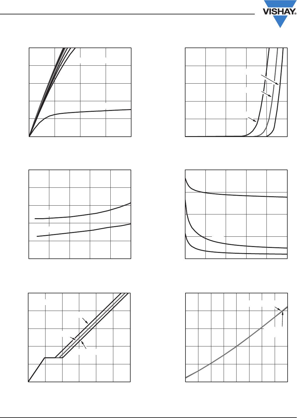
CHANNEL-1 TYPICAL CHARACTERISTICS 25 °C, unless otherwise noted
Output Characteristics
On-Resistance vs. Drain Current
Gate Charge
0
10
20
30
40
50
0.0 0.5 1.0 1.5 2.0
V
GS
=10Vthru4V
V
GS
=3V
V
DS
- Drain-to-Source Voltage (V)
- Drain Current (A)I
D
0.010
0.012
0.014
0.016
0.018
0.020
0 1020304050
V
GS
=10V
V
GS
=4.5V
- On-Resistance (Ω)R
DS(on)
I
D
- Drain Current (A)
0
2
4
6
8
10
0369121518
I
D
=9.5A
V
DS
=7.5V
V
DS
=24V
V
DS
=15V
- Gate-to-Source Voltage (V)
Q
g
- Total Gate Charge (nC)
V
GS
Transfer Characteristics
Capacitance
On-Resistance vs. Junction Temperature
0
2
4
6
8
10
0.0 0.6 1.2 1.8 2.4 3.0
T
C
= 25 °C
T
C
= 125 °C
T
C
= - 55 °C
V
GS
- Gate-to-Source Voltage (V)
- Drain Current (A)I
D
0
350
700
1050
1400
0 6 12 18 24 30
C
iss
C
oss
C
rss
V
DS
- Drain-to-Source Voltage (V)
C - Capacitance (pF)
0.7
0.9
1.1
1.3
1.5
1.7
- 50 - 25 0 25 50 75 100 125 150
V
GS
=4.5V
I
D
=8.7A
V
GS
=10V;I
D
=9.5A
T
J
- Junction Temperature (°C)
(Normalized)
- On-ResistanceR
DS(on)
Vishay Siliconix
Si4276DY
Document Number: 66599
S10-1289-Rev. A, 31-May-10
www.vishay.com
5
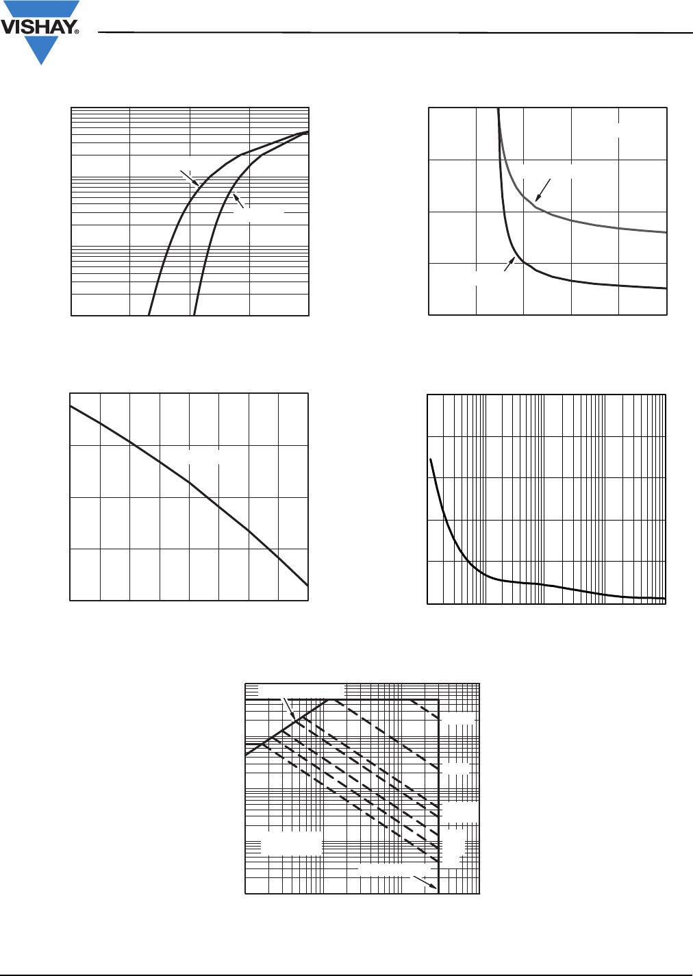
CHANNEL-1 TYPICAL CHARACTERISTICS 25 °C, unless otherwise noted
Source-Drain Diode Forward Voltage
Threshold Voltage
0.1
1
10
100
0.0 0.3 0.6 0.9 1.2
T
J
= 25 °C
T
J
= 150 °C
V
SD
- Source-to-Drain Voltage (V)
- Source Current (A)I
S
0.9
1.2
1.5
1.8
2.1
- 50 - 25 0 25 50 75 100 125 150
I
D
= 250 μA
(V)V
GS(th)
T
J
- Temperature (°C)
On-Resistance vs. Gate-to-Source Voltage
Single Pulse Power, Junction-to-Ambient
0.010
0.015
0.020
0.025
0.030
0246810
T
J
= 25 °C
I
D
=9.5A
T
J
= 125 °C
- On-Resistance (Ω)R
DS(on)
V
GS
- Gate-to-Source Voltage (V)
0.001
0
1
100
40
60
100.1
Time (s)
20
80
Power (W)
0.01
Safe Operating Area, Junction-to-Ambient
100
1
0.1 1 10 100
0.01
10
0.1
T
A
= 25 °C
Single Pulse
1s
10 s
Limited by R
DS(on)
*
BVDSS Limited
1ms
100 μs
10 ms
DC
100 ms
V
DS
- Drain-to-Source Voltage (V)
*V
GS
> minimum V
GS
at which R
DS(on)
is specied
- Drain Current (A)
I
D
www.vishay.com
6
Document Number: 66599
S10-1289-Rev. A, 31-May-10
Vishay Siliconix
Si4276DY
CHANNEL-1 TYPICAL CHARACTERISTICS 25 °C, unless otherwise noted
* The power dissipation P
D
is based on T
J(max)
= 150 °C, using junction-to-case thermal resistance, and is more useful in settling the upper
dissipation limit for cases where additional heatsinking is used. It is used to determine the current rating, when this rating falls below the package
limit.
Current Derating*
0
3
6
9
12
15
0 25 50 75 100 125 150
Package Limited
T
C
- Case Temperature (°C)
I
D
- Drain Current (A)
Power Derating, Junction-to-Foot
0
1
2
3
4
5
0 25 50 75 100 125 150
T
C
- Case Temperature (°C)
Power (W)
Power Derating, Junction-to-Ambient
0.0
0.3
0.6
0.9
1.2
1.5
0 25 50 75 100 125 150
T
A
- Ambient Temperature (°C)
Power (W)

SI4276DY-T1-GE3

Mfr. #:
Manufacturer:
Vishay / Siliconix
Description:
MOSFET RECOMMENDED ALT 781-SI4202DY-T1-GE3
Lifecycle:
New from this manufacturer.
Delivery:
DHL FedEx Ups TNT EMS
Payment:
T/T Paypal Visa MoneyGram Western Union

Products related to this Datasheet