Vishay Siliconix
Si4276DY
Document Number: 66599
S10-1289-Rev. A, 31-May-10
www.vishay.com
9
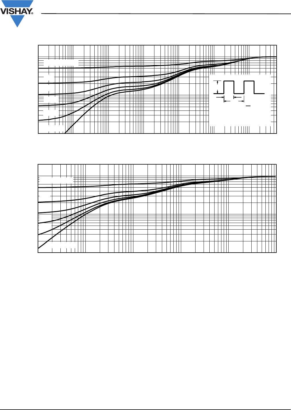
CHANNEL-2 TYPICAL CHARACTERISTICS 25 °C, unless otherwise noted
Source-Drain Diode Forward Voltage
Threshold Voltage
0.1
1
10
100
0.0 0.3 0.6 0.9 1.2
T
J
= 25 °C
T
J
= 150 °C
V
SD
- Source-to-Drain Voltage (V)
- Source Current (A)I
S
1.1
1.3
1.5
1.7
1.9
2.1
- 50 - 25 0 25 50 75 100 125 150
I
D
= 250 μA
(V)V
GS(th)
T
J
- Temperature (°C)
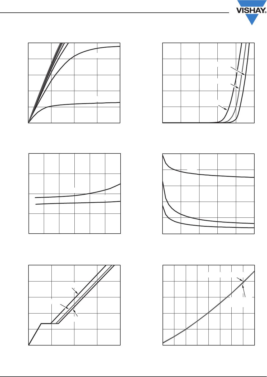
On-Resistance vs. Gate-to-Source Voltage
Single Pulse Power, Junction-to-Ambient
0
0.015
0.030
0.045
0.060
0246810
T
J
= 25 °C
I
D
=6.8A
T
J
= 125 °C
- On-Resistance (Ω)
R
DS(on)
V
GS
- Gate-to-Source Voltage (V)
0
10
20
30
40
50
Power (W)
Time (s)
10 10000.10.010.001 1001
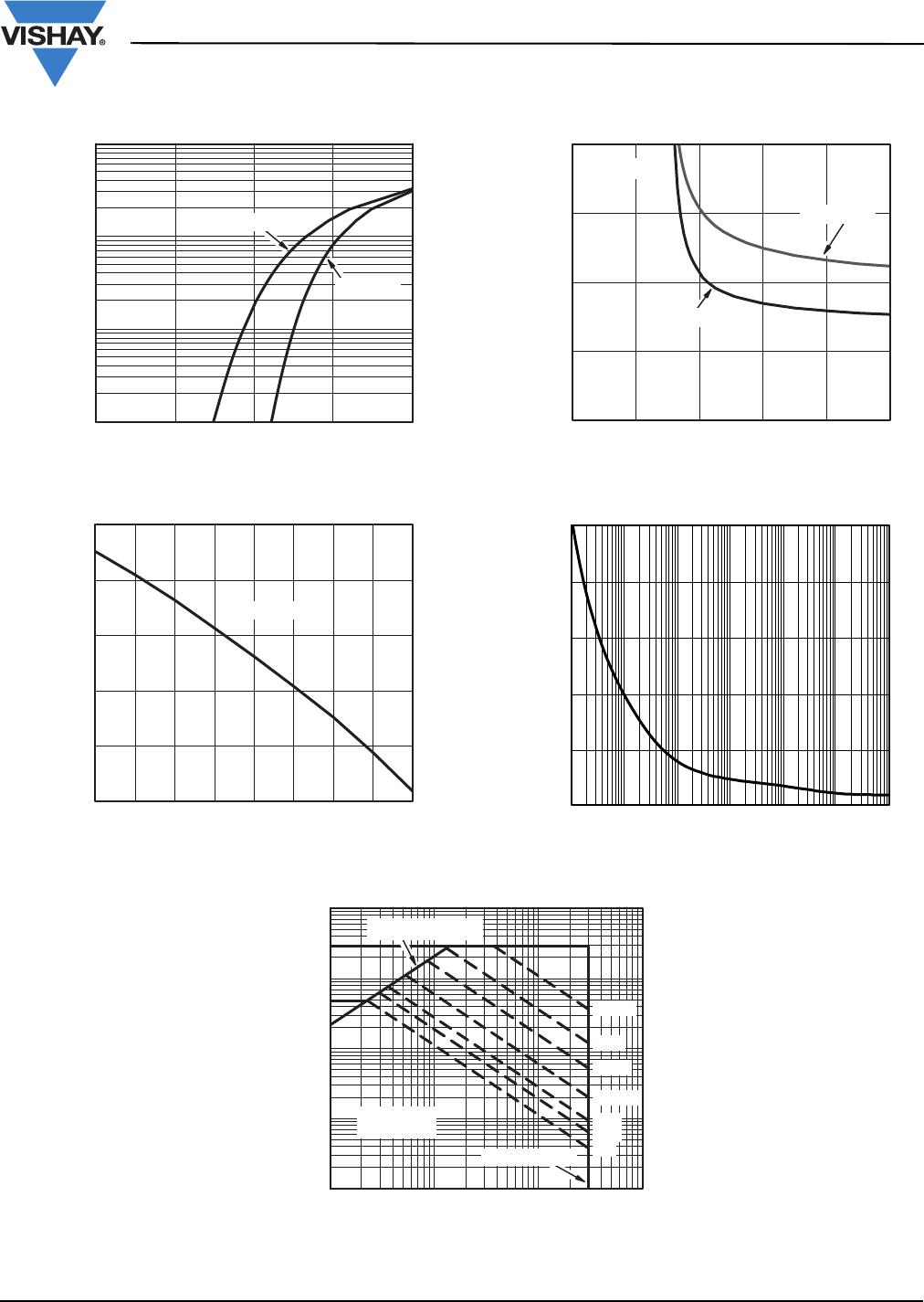
Safe Operating Area, Junction-to-Ambient
100
1
0.1 1 10 100
0.01
10
0.1
T
A
= 25 °C
Single Pulse
1s
10 s
Limited by R
DS(on)
*
BVDSS Limited
1ms
100 μs
10 ms
DC
100 ms
V
DS
- Drain-to-Source Voltage (V)
*V
GS
> minimum V
GS
at which R
DS(on)
is specied
- Drain Current (A)
I
D