LTC1860/LTC1861
13
18601fb
For more information www.linear.com/LTC1860
applicaTions inForMaTion
Reference Input
The reference input of the LTC1861 SO-8 package is
internally tied to V
CC
. The span of the A/D converter is
therefore equal to V
CC
. The voltage on the reference input
of the LTC1861 MSOP package defines the span of the
A/D converter. The LTC1861 MSOP package can operate
with reference voltages from 1V to V
CC
.
GENERAL ANALOG CONSIDERATIONS
Grounding
The LTC1860/LTC1861 should be used with an analog
ground plane and single point grounding techniques. Do not
use wire wrapping techniques to breadboard and evaluate
the device. To achieve the optimum performance, use a
printed circuit board. The ground pins (AGND and DGND
for the LTC1861 MSOP package and GND for the LTC1860
and LTC1861 SO-8 package) should be tied directly to the
analog ground plane with minimum lead length.
Bypassing
For good performance, the V
CC
and V
REF
pins must be free
of noise and ripple. Any changes in the V
CC
/V
REF
voltage
with respect to ground during the conversion cycle can
induce errors or noise in the output code. Bypass the V
CC
and V
REF
pins directly to the analog ground plane with a
minimum of 1µF tantalum. Keep the bypass capacitor
leads as short as possible.
Analog Inputs
Because of the capacitive redistribution A/D conversion
techniques used, the analog inputs of the LTC1860/
LTC1861 have capacitive switching input current spikes.
These current spikes settle quickly and do not cause a
problem if source resistances are less than 200Ω or high
speed op amps are used (e.g., the LT
®
1211, LT1469,
LT1807, LT1810, LT1630, LT1226 or LT1215). But if
large source resistances are used, or if slow settling op
amps drive the inputs, take care to ensure the transients
caused by the current spikes settle completely before the
conversion begins.
LTC1860/LTC1861
14
18601fb
For more information www.linear.com/LTC1860
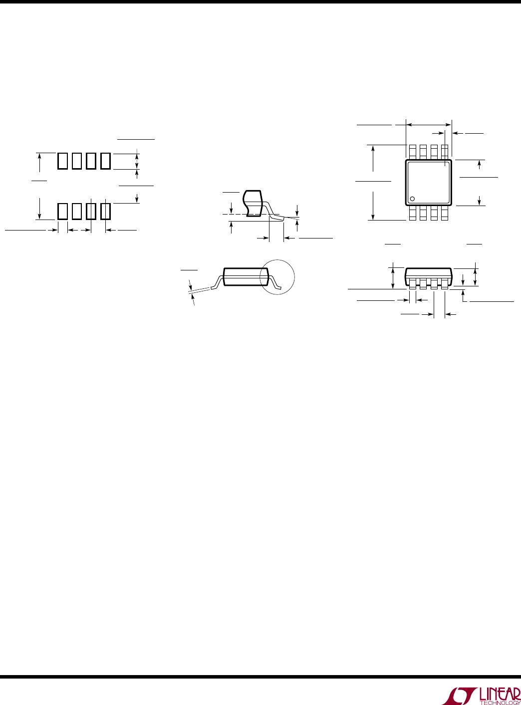
MS8 Package
8-Lead Plastic MSOP
(Reference LTC DWG # 05-08-1660 Rev F)
package DescripTion
MSOP (MS8) 0307 REV F
0.53 ± 0.152
(.021 ± .006)
SEATING
PLANE
NOTE:
1. DIMENSIONS IN MILLIMETER/(INCH)
2. DRAWING NOT TO SCALE
3. DIMENSION DOES NOT INCLUDE MOLD FLASH, PROTRUSIONS OR GATE BURRS.
MOLD FLASH, PROTRUSIONS OR GATE BURRS SHALL NOT EXCEED 0.152mm (.006") PER SIDE
4. DIMENSION DOES NOT INCLUDE INTERLEAD FLASH OR PROTRUSIONS.
INTERLEAD FLASH OR PROTRUSIONS SHALL NOT EXCEED 0.152mm (.006") PER SIDE
5. LEAD COPLANARITY (BOTTOM OF LEADS AFTER FORMING) SHALL BE 0.102mm (.004") MAX
0.18
(.007)
0.254
(.010)
1.10
(.043)
MAX
0.22 – 0.38
(.009 – .015)
TYP
0.1016 ± 0.0508
(.004 ± .002)
0.86
(.034)
REF
0.65
(.0256)
BSC
0° – 6° TYP
DETAIL “A”
DETAIL “A”
GAUGE PLANE
1 2
3
4
4.90 ± 0.152
(.193 ± .006)
8
7
6
5
3.00 ± 0.102
(.118 ± .004)
(NOTE 3)
3.00 ± 0.102
(.118 ± .004)
(NOTE 4)
0.52
(.0205)
REF
5.23
(.206)
MIN
3.20 – 3.45
(.126 – .136)
0.889 ± 0.127
(.035 ± .005)
RECOMMENDED SOLDER PAD LAYOUT
0.42 ± 0.038
(.0165 ± .0015)
TYP
0.65
(.0256)
BSC
Please refer to http://www.linear.com/product/LTC1860#packaging for the most recent package drawings.
LTC1860/LTC1861
15
18601fb
For more information www.linear.com/LTC1860
MS Package
10-Lead Plastic MSOP
(Reference LTC DWG # 05-08-1661 Rev E)
package DescripTion
MSOP (MS) 0307 REV E
0.53 ± 0.152
(.021 ± .006)
SEATING
PLANE
0.18
(.007)
1.10
(.043)
MAX
0.17 – 0.27
(.007 – .011)
TYP
0.86
(.034)
REF
0.50
(.0197)
BSC
1 2
3
4 5
4.90 ± 0.152
(.193 ± .006)
0.497 ± 0.076
(.0196 ± .003)
REF
8910
7
6
3.00 ± 0.102
(.118 ± .004)
(NOTE 3)
3.00 ± 0.102
(.118 ± .004)
(NOTE 4)
NOTE:
1. DIMENSIONS IN MILLIMETER/(INCH)
2. DRAWING NOT TO SCALE
3. DIMENSION DOES NOT INCLUDE MOLD FLASH, PROTRUSIONS OR GATE BURRS.
MOLD FLASH, PROTRUSIONS OR GATE BURRS SHALL NOT EXCEED 0.152mm (.006") PER SIDE
4. DIMENSION DOES NOT INCLUDE INTERLEAD FLASH OR PROTRUSIONS.
INTERLEAD FLASH OR PROTRUSIONS SHALL NOT EXCEED 0.152mm (.006") PER SIDE
5. LEAD COPLANARITY (BOTTOM OF LEADS AFTER FORMING) SHALL BE 0.102mm (.004") MAX
0.254
(.010)
0° – 6° TYP
DETAIL “A”
DETAIL “A”
GAUGE PLANE
5.23
(.206)
MIN
3.20 – 3.45
(.126 – .136)
0.889 ± 0.127
(.035 ± .005)
RECOMMENDED SOLDER PAD LAYOUT
0.305 ± 0.038
(.0120 ± .0015)
TYP
0.50
(.0197)
BSC
0.1016 ± 0.0508
(.004 ± .002)
Please refer to http://www.linear.com/product/LTC1861#packaging for the most recent package drawings.

LTC1860CS8#PBF

Mfr. #:
Manufacturer:
Analog Devices / Linear Technology
Description:
Analog to Digital Converters - ADC 12-bit, 250ksps ADC in MSOP
Lifecycle:
New from this manufacturer.
Delivery:
DHL FedEx Ups TNT EMS
Payment:
T/T Paypal Visa MoneyGram Western Union