LTC1860/LTC1861
7
18601fb
For more information www.linear.com/LTC1860
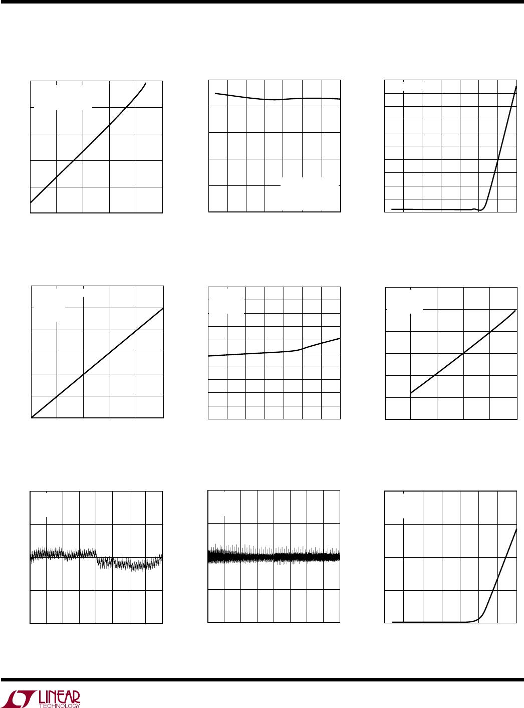
Typical perForMance cHaracTerisTics
Supply Current vs Sampling
Frequency
Supply Current vs Temperature
Sleep Current vs Temperature
Reference Current vs
Sample Rate
Reference Current vs
Temperature
Reference Current vs
Reference Voltage
Typical INL Curve
Typical DNL Curve
Analog Input Leakage vs
Temperature
SAMPLING FREQUENCY (kHz)
0.01
SUPPLY CURRENT (µA)
1000
100
10
1
0.1
0.01
100
1860/61 G01
0.1
1.0
10
1000
CONV LOW = 800ns
T
A
= 25°C
V
CC
= 5V
TEMPERATURE (°C)
–50
SUPPLY CURRENT (µA)
1000
800
600
400
200
0
0
50
75
1860/61 G02
–25
25
100
125
CONV HIGH = 3.2µS
f
SMPL
= 250kHz
V
CC
= 5V
V
REF
= 5V
TEMPERATURE (°C)
–50
SLEEP CURRENT (nA)
1000
900
800
700
600
500
400
300
200
100
0
0
50
75
1860/61 G03
–25
25
100
125
CONV = V
CC
= 5V
SAMPLE RATE (kHz)
0
REFERENCE CURRENT (µA)
60
50
40
30
20
10
0
50 100 150 200
1860/61 G04
250
CONV IS LOW FOR 800ns
T
A
= 25°C
V
CC
= 5V
V
REF
= 5V
TEMPERATURE (°C)
–50
REFERENCE CURRENT (µA)
55
54
53
52
51
50
49
48
47
46
45
0
50
75
1860/61 G05
–25
25
100
125
f
S
= 250kHz
V
CC
= 5V
V
REF
= 5V
V
REF
(V)
0
I
REF
(µA)
60
50
40
30
20
10
0
1 2 3 4
1860/61 G06
5
f
S
= 250kHz
T
A
= 25°C
V
CC
= 5V
CODE
0
INL COC ERROR (LSBs)
4096
1860/61 G07
1024
2048
3072
1.0
0.5
0
–0.5
–1.0
512 1536 2560
3584
T
A
= 25°C
V
CC
= 5V
V
REF
= 5V
CODE
0
DNL EOC ERROR (LSBs)
4096
1860/61 G07
1024
2048
3072
1.0
0.5
0
–0.5
–1.0
512 1536 2560
3584
T
A
= 25°C
V
CC
= 5V
V
REF
= 5V
TEMPERATURE (°C)
–50
ANALOG INPUT LEAKAGE (nA)
100
1860/61 G09
0 50
100
75
50
25
0
–25 25 75 125
V
CC
= 5V
V
REF
= 5V
CONV = 0V
LTC1860/LTC1861
8
18601fb
For more information www.linear.com/LTC1860
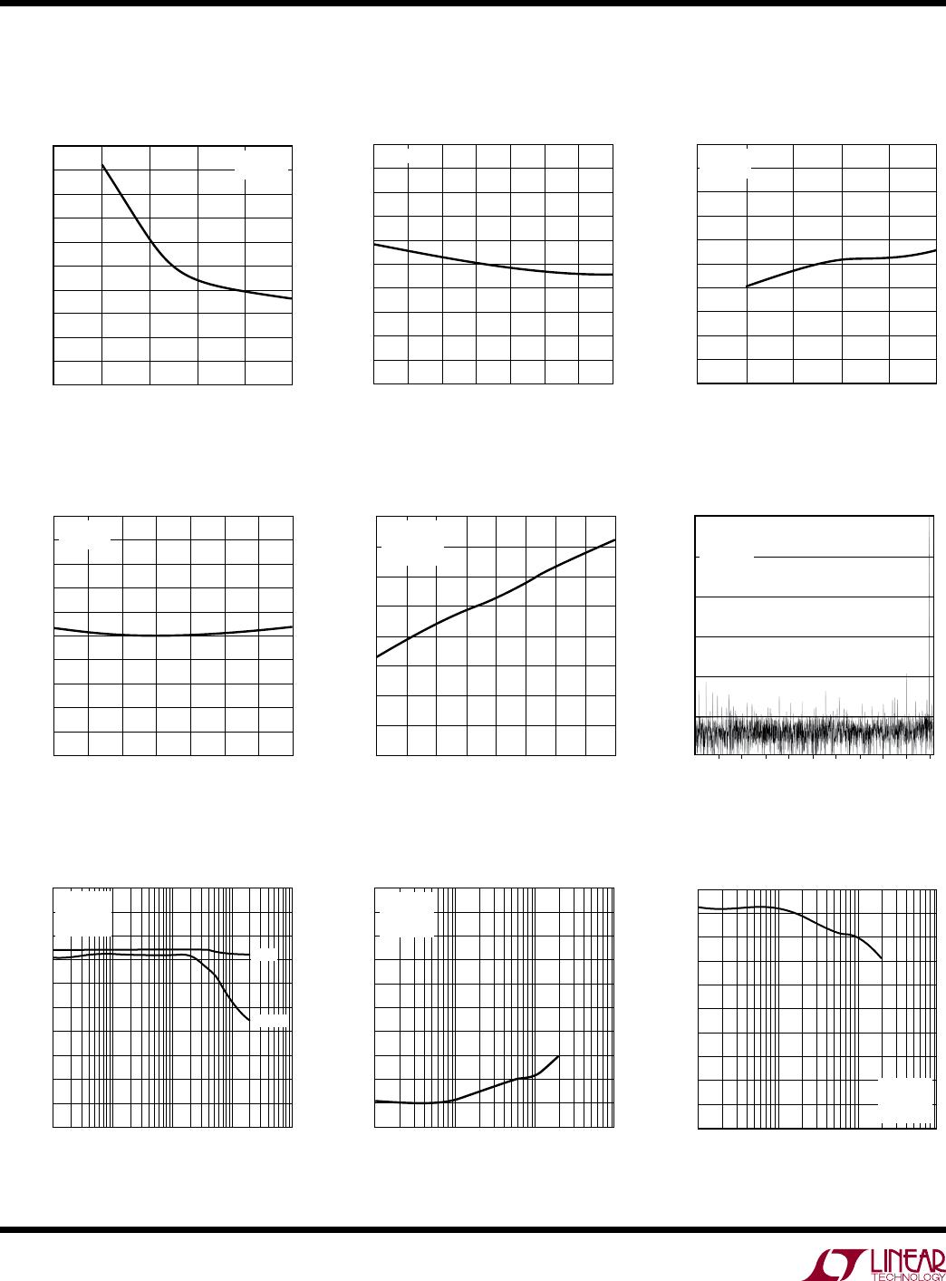
Typical perForMance cHaracTerisTics
Change in Offset Error vs
Reference Voltage
Change in Offset vs Temperature
Change in Gain Error vs
Reference Voltage
Change in Gain Error vs
Temperature
Signal-to-(Noise + Distortion)
vs Input Level
4096 Point FFT
Signal-to-(Noise + Distortion)
vs f
IN
Total Harmonic Distortion
vs f
IN
Spurious Free Dynamic Range
vs f
IN
REFERENCE VOLTAGE (V)
0
CHANGE IN OFFSET ERROR (LSB)
5
4
3
2
1
0
–1
–2
–3
–4
–5
4
1860/61 G10
1
2
3
5
T
A
= 25°C
V
CC
= 5V
TEMPERATURE (°C)
–50
CHANGE IN OFFSET (LSB)
1.0
0.8
0.6
0.4
0.2
0
–0.2
–0.4
–0.6
–0.8
–1.0
0
50
75
1860/61 G11
–25
25
100
125
V
CC
= 5V
REFERENCE VOLTAGE(V)
0
CHANGE IN GAIN ERROR (LSB)
5
4
3
2
1
0
–1
–2
–3
–4
–5
2
4
5
1860/61 G12
1
3
V
CC
= 5V
T
A
= 25°C
TEMPERATURE (°C)
–50
CHANGE IN GAIN ERROR (LSB)
1.0
0.8
0.6
0.4
0.2
0
–0.2
–0.4
–0.6
–0.8
–1.0
0
50
75
1860/61 G13
–25
25
100
125
V
CC
= 5V
V
REF
= 5V
INPUT LEVEL (dB)
–40
SIGNAL-TO-(NOISE + DISTORTION) (dB)
1195 G20
–30–35
–25
–15–20 –5–10 0
80
70
60
50
40
30
20
10
0
f
IN
= 10kHz
T
A
= 25°C
V
CC
= 5V
f (kHz)
0 60 70 90
AMPLITUDE (dB)
0
–20
–40
–60
–80
–100
–120
10 20 30 8040
1860/61 G15
10050
f
S
= 204.1kHz
f
IN
= 99.5kHz
T
A
= 25°C
V
CC
= 5V
f
IN
(kHz)
SIGNAL-TO-(NOISE + DISTORTION) (dB)
100
90
80
70
60
50
40
30
20
10
0
1 100 1000 10000
1860/61 G16
10
T
A
= 25°C
V
CC
= 5V
V
IN
= 0dB
SNR
SINAD
f
IN
(kHz)
1
TOTAL HARMONIC DISTORTION (dB)
0
–10
–20
–30
–40
–50
–60
–70
–80
–90
–100
10 100 1000
T
A
= 25°C
V
CC
= 5V
V
IN
= 0dB
f
IN
(kHz)
1
SPURIOUS FREE DYNAMIC RANGE (dB)
100
90
80
70
60
50
40
30
20
10
0
10 100 1000
T
A
= 25°C
V
CC
= 5V
V
IN
= 0dB
LTC1860/LTC1861
9
18601fb
For more information www.linear.com/LTC1860
pin FuncTions
LTC1860
V
REF
(Pin 1): Reference Input. The reference input defines
the span of the A/D converter and must be kept free of
noise with respect to GND.
IN
+
, IN
(Pins 2, 3): Analog Inputs. These inputs must be
free of noise with respect to GND.
GND (Pin 4): Analog Ground. GND should be tied directly
to an analog ground plane.
CONV (Pin 5): Convert Input. A logic high on this input
starts the A/D conversion process. If the CONV input is
left high after the A/D conversion is finished, the part
powers down. A logic low on this input enables the SDO
pin, allowing the data to be shifted out.
SDO (Pin 6): Digital Data Output. The A/D conversion
result is shifted out of this pin.
SCK (Pin 7): Shift Clock Input. This clock synchronizes
the serial data transfer.
V
CC
(Pin 8):
Positive Supply. This supply must be kept
free of noise and ripple by bypassing directly to the
analog ground plane.
LTC1861 (MSOP Package)
CONV (Pin 1): Convert Input. A logic high on this input
starts the A/D conversion process. If the CONV input is
left high after the A/D conversion is finished, the part
powers down. A logic low on this input enables the SDO
pin, allowing the data to be shifted out.
CH0, CH1 (Pins 2, 3): Analog Inputs. These inputs must
be free of noise with respect to AGND.
AGND (Pin 4): Analog Ground. AGND should be tied directly
to an analog ground plane.
DGND (Pin 5): Digital Ground. DGND should be tied directly
to an analog ground plane.
SDI (Pin 6):
Digital Data Input. The A/D configuration
word is shifted into this input.
SDO (Pin 7): Digital Data Output. The A/D conversion
result is shifted out of this output.
SCK (Pin 8): Shift Clock Input. This clock synchronizes
the serial data transfer.
V
CC
(Pin 9):
Positive Supply. This supply must be kept
free of noise and ripple by bypassing directly to the
analog ground plane.
V
REF
(Pin 10): Reference Input. The reference input defines
the span of the A/D converter and must be kept free of
noise with respect to AGND.
LTC1861 (SO-8 Package)
CONV (Pin 1): Convert Input. A logic high on this input
starts the A/D conversion process. If the CONV input is
left high after the A/D conversion is finished, the part
powers down. A logic low on this input enables the SDO
pin, allowing the data to be shifted out.
CH0, CH1 (Pins 2, 3): Analog Inputs. These inputs must
be free of noise with respect to GND.
GND (Pin 4): Analog Ground. GND should be tied directly
to an analog ground plane.
SDI (Pin 5):
Digital Data Input. The A/D configuration
word is shifted into this input.
SDO (Pin 6): Digital Data Output. The A/D conversion
result is shifted out of this output.
SCK (Pin 7): Shift Clock Input. This clock synchronizes
the serial data transfer.
V
CC
(Pin 8):
Positive Supply. This supply must be kept
free of noise and ripple by bypassing directly to the analog
ground plane. V
REF
is tied internally to this pin.
LTC1860CS8#PBF

Mfr. #:
Manufacturer:
Analog Devices / Linear Technology
Description:
Analog to Digital Converters - ADC 12-bit, 250ksps ADC in MSOP
Lifecycle:
New from this manufacturer.
Delivery:
DHL FedEx Ups TNT EMS
Payment:
T/T Paypal Visa MoneyGram Western Union