LTC1860/LTC1861
4
18601fb
For more information www.linear.com/LTC1860
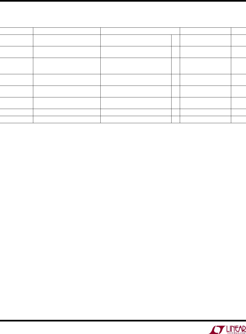
conVerTer anD MulTiplexer cHaracTerisTics
SYMBOL CONDITIONS MIN TYP MAX UNITS
Resolution
l
12 Bits
No Missing Codes Resolution
l
12 Bits
INL (Note 3)
l
±1 LSB
Transition Noise 0.07 LSB
RMS
Gain Error
l
±20 mV
Offset Error LTC1860 SO-8 and MSOP, LTC1861 MSOP
LTC1861 SO-8
l
l
±2
±3
±5
±7
mV
mV
Input Differential Voltage Range
V
IN
= IN
+
– IN
l
0 V
REF
V
Absolute Input Range IN
+
Input
IN
Input
–0.05
–0.05
V
CC
+ 0.05
V
CC
/2
V
V
V
REF
Input Range LTC1860 SO-8 and MSOP, LTC1861 MSOP 1 V
CC
V
Analog Input Leakage Current (Note 4)
l
±1 µA
C
IN
Input Capacitance In Sample Mode
During Conversion
12
5
pF
pF
The
l
denotes specifications which apply over the full operating temperature range, otherwise specifications are T
A
= 25°C.
V
CC
= 5V, V
REF
= 5V, f
SCK
= f
SCK(MAX)
as defined in Recommended Operating Conditions, unless otherwise noted.
DynaMic accuracy
SYMBOL PARAMETER CONDITIONS MIN TYP MAX UNITS
SNR Signal-to-Noise Ratio 72 dB
S/(N + D) Signal-to-Noise Plus Distortion Ratio 100kHz Input Signal 71 dB
THD Total Hamonic Distortion Up to 5th Harmonic 100kHz Input Signal 77 dB
Full Power Bandwidth 20 MHz
Full Linear Bandwidth S/(N + D) ≥ 68dB 125 kHz
T
A
= 25°C.
V
CC
= 5V, f
SAMPLE
= 250kHz, unless otherwise specified.
DigiTal anD Dc elecTrical cHaracTerisTics
SYMBOL PARAMETER CONDITIONS MIN TYP MAX UNITS
V
IH
High Level Input Voltage V
CC
= 5.25V
l
2.4 V
V
IL
Low Level Input Voltage V
CC
= 4.75V
l
0.8 V
I
IH
High Level Input Current V
IN
= V
CC
l
2.5 µA
I
IL
Low Level Input Current V
IN
= 0V
l
–2.5 µA
V
OH
High Level Output Voltage V
CC
= 4.75V, I
O
= 10µA
V
CC
= 4.75V, I
O
= 360µA
l
l
4.5
2.4
4.74
4.72
V
V
V
OL
Low Level Output Voltage V
CC
= 4.75V, I
O
= 1.6mA
l
0.4 V
The
l
denotes specifications which apply
over the full operating temperature range, otherwise specifications are T
A
= 25°C.
V
CC
= 5V, V
REF
= 5V, unless otherwise noted.
LTC1860/LTC1861
5
18601fb
For more information www.linear.com/LTC1860
DigiTal anD Dc elecTrical cHaracTerisTics
The
l
denotes specifications which apply
over the full operating temperature range, otherwise specifications are T
A
= 25°C.
V
CC
= 5V, V
REF
= 5V, unless otherwise noted.
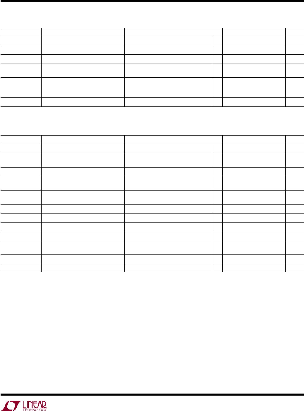
SYMBOL PARAMETER CONDITIONS MIN TYP MAX UNITS
I
OZ
Hi-Z Output Leakage CONV = V
CC
l
±3 µA
I
SOURCE
Output Source Current V
OUT
= 0V –25 mA
I
SINK
Output Sink Current V
OUT
= V
CC
20 mA
I
REF
Reference Current (LTC1860 SO-8,
MSOP and LTC1861 MSOP)
CONV = V
CC
f
SMPL
= f
SMPL(MAX)
l
l
0.001
0.05
3
0.1
µA
mA
I
CC
Supply Current CONV = V
CC
After Conversion
CONV = V
CC
After Conversion, H-Grade
f
SMPL
= f
SMPL(MAX)
l
l
l
0.001
0.001
0.85
3
5
1.3
µA
µA
mA
P
D
Power Dissipation f
SMPL
= f
SMPL(MAX)
1.25 mV
recoMMenDeD operaTing conDiTions
The
l
denotes specifications which apply over
the full operating temperature range, otherwise specifications are T
A
= 25°C.
SYMBOL PARAMETER CONDITIONS MIN TYP MAX UNITS
V
CC
Supply Voltage 4.75 5.25 V
f
SCK
Clock Frequency
H-Grade
l
l
20
16.7
MHz
MHz
t
CYC
Total Cycle Time 12 SCK + t
CONV
µs
t
SMPL
Analog Input Sampling Time LTC1860 (Note 5)
LTC1861 (Note 5)
12
10
SCK
SCK
t
suCONV
Setup Time CONV Before First SCK,
(See Figure 1)
H-Grade
60
65
30
30
ns
ns
t
hDI
Holdtime SDI After SCK LTC1861 15 ns
t
suDI
Setup Time SDI Stable Before SCK LTC1861 15 ns
t
WHCLK
SCK High Time f
SCK
= f
SCK(MAX)
40% 1/f
SCK
t
WLCLK
SCK Low Time f
SCK
= f
SCK(MAX)
40% 1/f
SCK
t
WHCONV
CONV High Time Between Data Transfer
Cycles
(Note 5) t
CONV
µs
t
WLCONV
CONV Low Time During Data Transfer (Note 5) 12 SCK
t
hCONV
Hold Time CONV Low After Last SCK 13 ns
LTC1860/LTC1861
6
18601fb
For more information www.linear.com/LTC1860
Note 1: Stresses beyond those listed under Absolute Maximum Ratings
may cause permanent damage to the device. Exposure to any Absolute
Maximum Rating condition for extended periods may affect device
reliability and lifetime.
Note 2: All voltage values are with respect to GND.
Note 3: Integral nonlinearity is defined as deviation of a code from a
straight line passing through the actual endpoints of the transfer curve.
The deviation is measured from the center of the quantization band.
Note 4: Channel leakage current is measured while the part is in sample
mode.
Note 5: Guaranteed by design, not subject to test.
SYMBOL PARAMETER CONDITIONS MIN TYP MAX UNITS
t
CONV
Conversion Time (See Figure 1)
H-Grade
l
l
2.75
2.75
3.2
3.3
µs
µs
f
SMPL(MAX)
Maximum Sampling Frequency
H-Grade
l
l
250
248
kHz
kHz
t
dDO
Delay Time, SCK to SDO Data Valid C
LOAD
= 20pF
C
LOAD
= 20pF
C
LOAD
= 20pF, H-Grade
l
l
15 20
25
30
ns
ns
ns
t
dis
Delay Time, CONV to SDO Hi-Z
H-Grade
l
l
30
30
60
65
ns
ns
t
en
Delay Time, CONV to SDO Enabled C
LOAD
= 20pF
C
LOAD
= 20pF, H-Grade
l
l
30
30
60
65
ns
ns
t
hDO
Time Output Data Remains Valid After
SCK
C
LOAD
= 20pF
l
5 10 ns
t
r
SDO Rise Time C
LOAD
= 20pF 8 ns
t
f
SDO Fall Time C
LOAD
= 20pF 4 ns
TiMing cHaracTerisTics
The
l
denotes specifications which apply over the full operating temperature
range, otherwise specifications are T
A
= 25°C.
V
CC
= 5V, V
REF
= 5V, f
SCK
= f
SCK(MAX)
as defined in Recommended Operating
Conditions, unless otherwise noted.

LTC1860CS8#PBF

Mfr. #:
Manufacturer:
Analog Devices / Linear Technology
Description:
Analog to Digital Converters - ADC 12-bit, 250ksps ADC in MSOP
Lifecycle:
New from this manufacturer.
Delivery:
DHL FedEx Ups TNT EMS
Payment:
T/T Paypal Visa MoneyGram Western Union