AD1893
REV. A
–9–
AMP
TIME
SUBFILTER COEFFICIENTS
ALIGNED TO THE LEFT
T
SIN
= 1/F
SIN
FREQ
F
SIN
/2
F
SIN
/2
F
SIN
/2
F
SIN
/2
F
SIN
/2
PHASE
DELAY = NOMINAL
DELAY = NOMINAL
DELAY = NOMINAL – .25/F
SIN
DELAY = NOMINAL – .5/F
SIN
DELAY = NOMINAL – .75/F
SIN
Figure 3. Four Polyphase Subfilters Realigned to Coarse Time Grid
POLYPHASE FILTER 1
POLYPHASE FILTER 2
POLYPHASE FILTER 3
POLYPHASE FILTER 4
POLYPHASE FILTER 5
POLYPHASE FILTER 6
POLYPHASE FILTER 7
INPUT
SIGNAL
POLYPHASE FILTER N-1
POLYPHASE FILTER N
SELECT
N TO 1
MUX
OUTPUT
SIGNAL
SAMPLE
CLOCK
TRACKING
CIRCUIT
Figure 4. Polyphase Filter Bank Model—Conceptual Block
Diagram
The full set of subfilters can be considered to form a parallel
bank of “polyphase” filters which have decrementing, linear
phase group delays. All of the polyphase filters conceptually
process the input signal simultaneously, as illustrated in Figure
4, at the input sample rate.
Asynchronous sample rate conversion under the polyphase filter
bank model is accomplished by selecting the output of a particu-
lar polyphase filter on the basis of the temporal relationship
between the input sample clock and the output sample clock
events. Figure 5 shows the desired filter group delay as a func-
tion of the relative time difference between the current output
sample clock and the last input sample clock. If an output
sample is requested late in the input sample period, then a short
filter delay is required, and if an output sample is requested
early in the input sample period, then a long filter delay is re-
quired. This nonintuitive result arises from the fact that FIR
filters always produce some delay, so that selecting a filter with
shorter delay moves the interpolated sample closer to the newest
input sample.
AD1893
–10–
REV. A
AB
OUTPUT SEQUENCE
PAST
FUTURE
AMPLITUDE
AMPLITUDE
SHORT
DELAY
LONG
DELAY
SMALL
OFFSET
LARGE
OFFSET
OFFSET INTO DENSE FIR FILTER COEFFICIENT ARRAY
TO ACCESS REQUIRED POLYPHASE FILTER
REQUIRED FILTER GROUP DELAY TO
COMPUTE REQUESTED OUTPUT SAMPLE
INPUT SEQUENCE
Figure 5. Input and Output Clock Event Relationship
A short delay corresponds to a large offset into the dense FIR
filter coefficient array, and a long delay corresponds to a small
offset. Note that because the output sample clock can arrive at
any arbitrary time with respect to the input sample clock, the
selection of a polyphase filter with which to convolve the input
sequence occurs on every output sample clock event. Occasion-
ally the FIFO which holds the input sequence in the FIR con-
volver is either not incremented, or incremented by two between
output sample clocks (see periods A and B in Figure 5); this
happens more often when the input and output sample clock
frequencies are dissimilar than when they are close together.
However, in this situation, an appropriate polyphase filter is
selected to process the input signal, and thus an accurate output
sample is computed. Input and output samples are not skipped
or repeated (unless the input FIFO underflows or overflows), as
is the case in some other sample rate converter implementations.
To obtain an accurate conversion, a large number of polyphase
filters are needed. The AD1893 SamplePort uses the equivalent
of 65,536 polyphase filters to achieve its high quality distortion
and dynamic range specifications.
Sample Clock Tracking
It should be clear that, in either model, the correct computation
of the ratio between the input sample rate (as determined from
the left/right input clock, LR_I) and the output sample rate (as
determined from the left/right output clock, LR_O) is critical to
the quality of the output data stream. It is straightforward to
compute this ratio if the sample rates are fixed and synchronous;
the challenge is to accurately track dynamically varying and
asynchronous sample rates, as well as to account for jitter.
The AD1893 SamplePort solves this problem by embedding the
ratio computation circuit within a digital servo control loop, as
shown in Figure 6. This control loop includes special provisions
to allow for the accurate tracking of dynamically changing
sample rates. The outputs of the control loop are the starting
read addresses for the input data FIFO and the filter coefficient
ROM. These start addresses are used by the FIFO and ROM
address generators, as shown in Figure 6.
The input data FIFO write address is generated by a counter
which is clocked by the input sample clock (i.e., LR_I). It is very
important that the FIFO read address and the FIFO write ad-
dress do not cross, as this means that the FIFO has either
underflowed or overflowed. This consideration affects the
choice of settling time of the control loop. When a step change
in the sample rate occurs, the relative positions of the read and
write addresses will change while the loop is settling. A fast
settling loop will act to keep the FIFO read and write addresses
separated better than a slow settling loop. The AD1893 includes
a user selectable pin (SETLSLW) to set the loop settling time
that essentially changes the coefficients of the digital servo con-
trol loop filter. The state of the SETLSLW pin can be changed
on-the-fly but is normally set and forgotten.
FIFO WRITE
ADDRESS
GENERATOR
FIFO
SERIAL DATA
INPUT UNIT
FIFO READ
ADDRESS
GENERATOR
ACCUMULATOR
SERIAL DATA
OUTPUT UNIT
SAMPLE CLOCK RATIO
SERVO CONTROL LOOP
POLYPHASE
COEFFICIENT
ROM
ROM ADDRESS
GENERATOR
POLYPHASE FILTER
SELECTOR
DATA_I
LR_I
LR_O
WCLK_O
BCLK_O
WCLK_I
BCLK_I
FIR CONVOLVER
DATA_O
START
ADDRESS
FREQUENCY
RESPONSE
COMPRESSION
F
SOUT
< F
SIN
LR_I
(F
SIN
)
LR_O
(F
SOUT
)
LR_I
LR_I LR_O
Figure 6. Functional Block Diagram
AD1893
REV. A
–11–
Sample Clock Jitter Rejection
The loop filter settling time also affects the ability of the
AD1893 ASRC to reject sample clock jitter, since the control
loop effectively computes a time weighted average or “esti-
mated” new output of many past input and output clock events.
This first order low pass filtering of the sample clock ratio pro-
vides the AD1893 with its jitter rejection characteristic. In the
slow settling mode, the AD1893 attenuates jitter frequencies
higher than 3 Hz (800 ms for the control loop to settle to an
18-bit “pure” sine wave), and thus rejects all but the most se-
vere sample clock jitter; performance is essentially limited only
by the FIR filter. In the fast settling mode, the ASRC attenuates
jitter components above 12 Hz (200 ms for the control loop to
settle). Due to the effects of on-chip synchronization of the
sample clocks to the 16 MHz (62.5 ns) crystal master clock,
sample clock jitter must be a large percentage of the crystal
period (>10 ns) before performance degrades in either the slow
or fast settling modes. Note that since both past input and past
output clocks are used to compute the filtered “current” internal
output clock request, jitter on both the input sample clock and
the output sample clock is rejected equally. In summary: the fast-
settling mode is best for applications when the sample rates will
be dynamically altered (e.g., varispeed situations), while the
slow-settling mode provides the most sample clock jitter rejection.
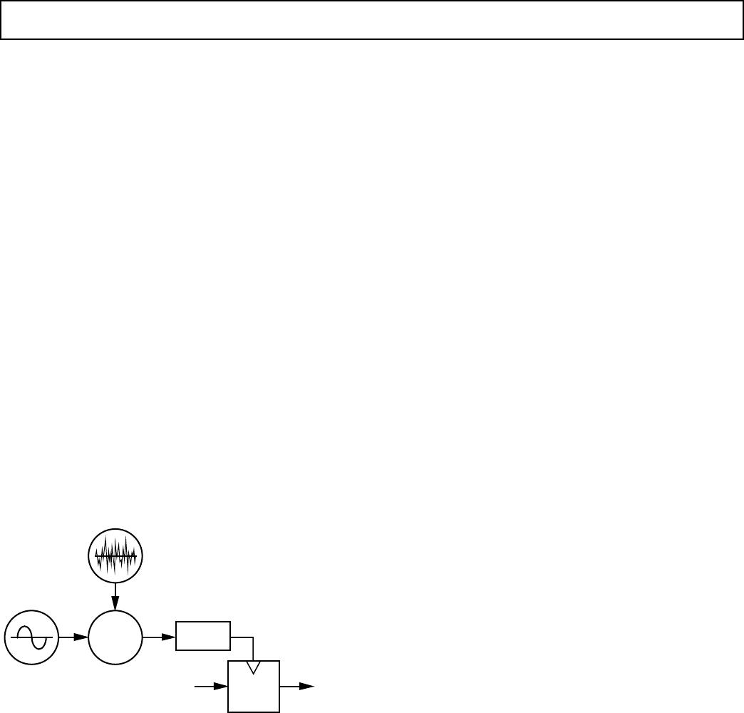
Clock jitter can be modeled as a frequency modulation process.
Figure 7 shows one such model, where a noise source combined
with a sine wave source modulates the “carrier” frequency gen-
erated by a voltage controlled oscillator.
NOISE SOURCE
VCO
DIGITAL
OUT
ANALOG IN
ADC
VOLTAGE
SOURCE
Σ
NOISE
WAVEFORM
SINE
WAVE
Figure 7. Clock Jitter Modeled as a Modulated VCO
If the jittered output of the VCO is used to clock an analog-to-
digital converter, the digital output of the ADC will be contami-
nated by the presence of jitter. If the noise source is spectrally
flat (i.e., “white” jitter), an FFT of the ADC digital output
would show a spectrum with a uniform noise floor that is
elevated compared to the spectrum with the noise source turned
off. If the noise source has distinct frequency components (i.e.,
“correlated” jitter), then an FFT of the ADC digital output
would show symmetrical sidebands around the ADC input
signal, at amplitudes and frequencies determined by frequency
modulation theory. One notable result is that the level of the
noise or the sidebands is proportional to the slope of the input
signal, i.e., the worst case occurs at the highest frequency full-
scale input (a full-scale 20 kHz sinusoid).
The AD1893 applies rejection to these jitter frequency compo-
nents referenced to the input signal. In other words, if a 5 kHz
digital sinusoid is applied to the ASRC, depending on the set-
tling mode selected, the ASRC will attenuate sample clock jitter
at either 3 Hz above and below 5 kHz (slow settling) or 12 Hz
above and below 5 kHz (fast settling). The rolloff is 6 dB per
octave. As an example, suppose there was correlated jitter
present on the input sample clock with a 1 kHz component,
associated with the same 5 kHz sinusoidal input data. This
would produce sidebands at 4 kHz and 6 kHz, 3 kHz and
7 kHz, etc., with amplitudes that decrease as they move away
from the input signal frequency. For the slow-settling mode
case, 1 kHz represents more than nine octaves (relative to
3 Hz), so the first two sideband pairs would be attenuated by
more than 54 dB. For the fast-settling mode case, 1 kHz repre-
sents more than seven octaves (relative to 12 Hz), so that the
first two sideband pairs would be attenuated by more than 42 dB.
The second and higher sideband pairs are attenuated even more
because they are spaced further from the input signal frequency.
Group Delay Modes
The other parameter that determines the likelihood of FIFO
input overflow or output underflow is the FIFO depth. This
FIFO induced group delay is better termed transport delay,
since it is frequency independent, and should be kept conceptu-
ally distinct from the notion of group delay as used in the poly-
phase filter bank model. The total group delay of the AD1893
equals the FIFO transport delay plus the FIR (polyphase) filter
group delay.
In the AD1893, the FIFO read and write pointers are separated
by five memory locations (100 µs equivalent transport delay at
a 50 kHz sample rate). This is added to the FIR filter delay
(64 taps divided by 2) for a total nominal group delay in short
mode of 700 µs.
This delay is deterministic and constant except when F
SOUT
drops below F
SIN
which causes the number of FIR filter taps to
increase (see Cutoff Frequency Modification section). If the
FIFO read and write addresses cross, the MUTE_O signal will
be asserted. Note that under all conditions, both the highly
oversampled low-pass prototype and the polyphase subfilters of
the AD1893 ASRC possess a linear phase response.

AD1893JSTZ

Mfr. #:
Manufacturer:
Description:
Audio Sample Rate Converters IC SamplePort 16-Bit ASRC
Lifecycle:
New from this manufacturer.
Delivery:
DHL FedEx Ups TNT EMS
Payment:
T/T Paypal Visa MoneyGram Western Union

Products related to this Datasheet