AD1893
–12–
REV. A
Cutoff Frequency Modification
The final important operating concept of the ASRC is the modi-
fication of the filter cutoff frequency when the output sample
rate (F
SOUT
) drops below the input sample rate (F
SIN
), i.e.,
during downsampling operation. The AD1893 automatically
reduces the polyphase filter cutoff frequency under this condi-
tion. This lowering of the cutoff frequency (i.e., the reduction of
the input signal bandwidth) is required to avoid alias distortion.
The AD1893 SamplePort takes advantage of the scaling prop-
erty of the Fourier transform which can be stated as follows: if
the Fourier transform of f(t) is F(w), then the Fourier transform
of f(k × t) is F(w/k). This property can be used to linearly com-
press the frequency response of the filter, simply by multiplying
the coefficient ROM addresses (shown in Figure 6) by the ratio
of F
SOUT
to F
SIN
whenever F
SOUT
is less than F
SIN
. This scaling
property works without spectral distortion because the time scale
of the interpolated signal is so dense (300 ps resolution) with
respect to the cutoff frequency that the discrete-time representa-
tion is a close approximation to the continuous time function.
The cutoff frequency (–3 dB down) of the FIR filter during
downsampling is given by the following relation:
Downsampling Cutoff Frequency = (F
SOUT
/44.1 kHz) × 20 kHz
The AD1893 frequency response compression circuit includes a
first order low-pass filter to smooth the filter cutoff frequency
selection during dynamic sample rate conditions. This allows
the ASRC to avoid objectionable clicking sounds that would
otherwise be imposed on the output while the loop settles to a
new sample rate ratio. Hysteresis is also applied to the filter
selection with approximately 300 Hz of cutoff frequency “noise
margin,” which limits the available selection of cutoff frequen-
cies to those falling on an approximately 300 Hz frequency grid.
Thus if a particular sample frequency ratio was reached by slid-
ing the output sample frequency up, it is possible that a filter
will be chosen with a cutoff frequency that could differ by as
much as 300 Hz from the filter chosen when the same sample
frequency ratio was reached by sliding the output sample fre-
quency down. This is necessary to ensure that the filter selection
is stable even with severely jittered input sample clocks.
Note that when the filter cutoff frequency is reduced, the transi-
tion band of the filter becomes narrower since the scaling prop-
erty affects all filter characteristics. The number of FIR filter
taps necessarily increases because there are now a smaller num-
ber of longer length polyphase filters. Nominally, when F
SOUT
is
greater than F
SIN
, the number of taps is 64. When F
SOUT
is less
than F
SIN
, the number of taps linearly increase to a maximum
of 128 when the ratio of F
SOUT
to F
SIN
equals 1:2. The number
of filter taps as a function of sample clock ratio is illustrated in
Figure 8. The natural consequence of this increase in filter taps
is an increase in group delay.
0.5 1.0 1.5 2.0
NUMBER OF FILTER TAPS
128
64
F
SOUT
/F
SIN
UPSAMPLING
DOWN-
SAMPLING
Figure 8. Number of Filter Taps as a Function of F
SOUT
/F
SlN
When the AD1893 output sample frequency is higher than the
input sample frequency (i.e., upsampling operation), the cutoff
frequency of the FIR polyphase filter can be greater than 20 kHz.
The cutoff frequency of the FIR filter during upsampling is
given by the following relation:
Upsampling Cutoff Frequency = (F
SIN
/44.1 kHz) × 20 kHz
Noise and Distortion Phenomena
There are three noise/distortion phenomena that limit the per-
formance of the AD1893 ASRC. First, there is broadband,
Gaussian noise that results from polyphase filter selection
quantization. Even though the AD1893 has a large number of
polyphase filters (the equivalent of 65,536) from which to
choose, the selection is not infinite. Second, there is narrowband
noise that results from the nonideal synchronization of the
sample clocks to the 16 MHz system clock, which leads to a
nonideal computation of the sample clock ratio, which leads
to a nonideal polyphase filter selection. This noise source is
narrowband because the digital servo control loop averages the
polyphase filter selection, leading to a strong correlation be-
tween selections from output to output. In slow mode, the selec-
tion of polyphase filters is completely unaffected by the clock
synchronization. In fast mode, some narrowband noise modula-
tion may be observed with very long FFT measurements. This
situation is analogous to the behavior of a phase locked loop
when presented with a noisy or jittered input. Third, there are
distortion components that are due to the noninfinite stopband
rejection of the low-pass filter response. Noninfinite stopband
rejection means that some amount of out-of-band spectral en-
ergy will alias into the baseband. The AD1893 performance
specifications include the effects of these phenomena.
Note that Figures 16 through 18 are shown with full-scale input
signals. The distortion and noise components will scale with the
input signal amplitude. In other words, if the input signal is
attenuated by –20 dB, the distortion and noise components will
also be attenuated by –20 dB. This dependency holds until the
effects of the 16-bit input quantization are reached.
AD1893
REV. A
–13–
OPERATING FEATURES
Serial Input/Output Ports
The AD1893 uses the frequency of the left/right input clock
(LR_ I) and the left/right output clock (LR_O) signals to deter-
mine the sample rate ratio, and therefore these signals must run
continuously and transition twice per sample period. (The LR_I
clock frequency is equivalent to F
SIN
and the LR_O clock fre-
quency is equivalent to F
SOUT
.) The other clocks (WCLK_I,
WCLK_O, BCLK_I, BCLK_O) are edge sensitive and may be
used in a gated or burst mode (i.e., a stream of pulses during
data transmission or reception followed by periods of inactivity).
The word clocks and the output bit clock are used only to write
data into or read data out of the serial ports; only the left/right
clocks are used in the internal DSP blocks. The input bit clock
is used to sample the input left/right clock. It is important that
the left/right clocks are “clean” with monotonic rising and falling
edge transitions and no excessive overshoot or undershoot which
could cause false triggering on the AD1893.
The AD1893’s flexible serial input and output ports consume
and produce data in twos-complement, MSB-first format. The
left channel data field always precedes the right channel data
field; the current channel being consumed or produced is indi-
cated by the state of the left/right clock (LR_I and LR_O). A left
channel field, right channel field pair is called a frame. The
input data field consists of 4 to 16 bits. The output data field
consists of 4 to 24 bits. The input signals are specified to TTL
logic levels, and the outputs swing to full CMOS logic levels.
The ports are configured by pin selections.
Serial I/O Port Modes
The AD1893 has pin-selectable bit clock polarity for the input
and output ports. In “normal” mode (BKPOL_I or BKPOL_O
LO) the data is valid on the rising edge. In the “inverted” mode
(BKPOL_I or BKPOL_O HI) the data is valid on the falling
edge. Both modes are shown in Figures 23 and 24.
The AD1893 uses two multiplexed input pins to control the mode
configuration of the input and output serial ports. MODE0_I
and MODE1_I control the input serial port, and MODE0_O
and MODE1_O control the output serial port as follows:
MODE0_I MODE1_I Serial Input Port Mode
0 0 Left-justified, no MSB delay, LR_I clock
triggered.
0 1 Left-justified, MSB delay, LR_I clock
triggered.
1 0 Right-justified, MSB delayed 16-bit clock
periods from LR_I clock transition, LR_I
clock triggered.
1 1 Word clock triggered, no MSB delay.
MODE0_O MODE1_O Serial Output Port Mode
0 0 Left-justified, no MSB delay, LR_O clock
triggered.
0 1 Left-justified, MSB delay, LR_O clock
triggered.
1 0 Right-justified, MSB delayed 16-bit clock
periods from LR_O clock transition, LR_O
clock triggered.
1 1 Word clock triggered, no MSB delay.
The MSB delay is useful for I
2
S format compatibility and for
ease of interfacing to some DSP processors.
The AD1893 SamplePort serial ports operate in either the word
clock (WCLK_I, WCLK_O) triggered mode or left/right clock
(LR_I, LR_O) triggered mode. These modes can be utilized
independently for the input and output ports. In the word clock
triggered mode, as shown in Figure 23, after the left/right clock
is valid, the appearance of the MSB of data is synchronous with
the rising edge of the word clock. Note that the word clock is
rising edge sensitive, and can fall anytime after it is sampled HI
by the bit clock. In the left-justified left/right clock triggered
modes, as shown in Figure 24, the appearance of the MSB of
data is synchronous with the rising edge of the left/right clock
for the left channel and the falling edge of left/right clock for the
right channel. The MSB is delayed by one bit clock after the
left/right clock if the MSB delay mode is selected. In the right-
justified left/right clock triggered mode, as shown in Figure 25,
the MSB is delayed 16 bit clock periods from a left/right clock
edge, so that when there are 64 bit clock periods per frame, the
LSB is right-justified to a left/right clock edge. The word clock
is not required in the left/right clock triggered modes, and
should be tied either HI or LO. Figure 24 shows the bit clock in
the optional gated or burst mode; the bit clock is inactive be-
tween data fields, and can take either the HI state or the LO
state while inactive.
Note that there is no requirement for a delay between the left
channel data and the right channel data. The left/right clocks
and the word clocks can transition immediately after the LSB of
the data, so that the MSB of the subsequent channel appears
without any timing delay. The AD1893 is therefore capable of a
32-bit frame mode, in which both 16-bit channels are packed
into a 32-bit clock period. More generally, there is no particular
requirement for when the left/right clock falls (i.e., there is no
left/right clock duty cycle or pulsewidth specification), provided
that the left/right clock frequency equals the intended sample
frequency, and there are sufficient bit clock periods to clock in
or out the intended number of data bits.
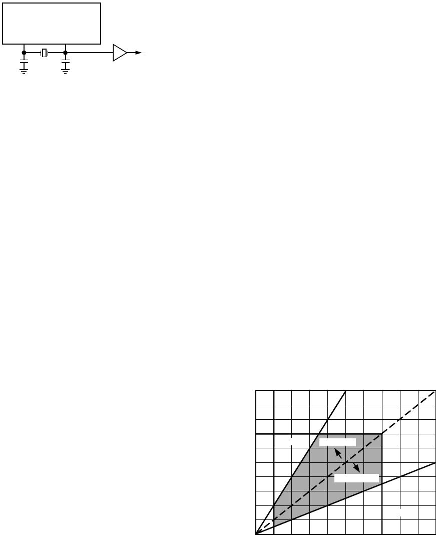
On-Chip Oscillator
The AD1893 includes an on-chip oscillator so that the user
need only supply an external quartz crystal or ceramic resonator.
The crystal or the resonator should be tied to the XTAL_I and
XTAL_O pins of the AD1893. An external crystal oscillator can
be used to overdrive the AD1893 on-chip oscillator. The exter-
nal clock source should be applied to the XTAL_I pin, and the
XTAL_O pin should be left unconnected.
Figure 9. Crystal and Oscillator Connections
AD1893
–14–
REV. A
Some applications using multiple AD1893s may desire to use
the same master clock frequency for all the SamplePorts, sup-
plied by a single crystal. The crystal output can be buffered with
a 74HCXX gate and distributed to the other XTAL_I inputs, as
shown in Figure 10.
AD1893
XTAL_I XTAL_O
16MHz
20pF 15pF
74HC DEVICE
TO XTAL_I
INPUTS
Figure 10. Buffered 16 MHz Crystal Connection
Power-Down Mode
The AD1893 includes a power-down control input pin
PWRDWN. This control signal is active HI, and puts the
AD1893 in an inactive state with very low power dissipation.
The PWRDWN pin should be connected LO when normal
operation of the AD1893 is desired.
Control Signals
The SETLSLW, BKPOL_I, BKPOL_O, MODE0_I, MODE1_I,
MODE0_O and MODE1_O inputs are asynchronous signals in
that they need obey no particular timing relation to the crystal
frequency or the sample clocks. Ordinarily, these pins are hard-
wired or connected to an I/O register for microprocessor control.
The only timing requirement on these pins is that the control
signals are stable and valid before the first serial input data bit
(i.e., the MSB) is presented to the AD1893.
Reset
Figure 27 shows the reset timing for the AD1893 SamplePort. A
crystal (or resonator) must be connected to the AD1893 when
RESET is asserted, and the bit clocks, the word clocks and the
left/right clocks may also be running. When the AD1893 comes
out of reset, it defaults to a F
SIN
to F
SOUT
ratio of 1:1. The filter
pipeline is not cleared. However, the mute output goes HI for at
least 128 cycles, adequate to allow the pipeline to clear. If F
SIN
differs significantly from F
SOUT
, then the AD1893 sample clock
servo control loop also has to settle. While settling, the mute
output will be HI. After the external system resets the AD1893,
it should wait until the mute output goes LO before clocking in
serial data.
There is no requirement for using the RESET pin at power-up
or when the input or output sample rate changes. If it is not
used, the AD1893 will settle to the sample clocks supplied within
200 ms in fast-settling mode or within 800 ms in slow-settling
mode.
APPLICATION ISSUES
Dither
Due to the large output word length, no redithering of the
AD1893 output is necessary. This assumes that the input is
properly dithered and the user retains the same or greater num-
ber of output bits as there are input bits. The AD1893 output
bit stream may thus be used directly as the input to downstream
digital audio processors, storage media or output devices.
If the AD1893 is to be used to dramatically downsample (i.e.,
output sample frequency is much lower than input sample fre-
quency), the input should be sufficiently dithered to account for
the limiting of the input signal bandwidth (which reduces the
rms level of the input dither). No dither is internally used or
applied to the audio data in the AD1893 SamplePort.
Decoupling and PCB Layout
The AD1893 ASRC has two power and two ground connections to
minimize output switching noise and ground bounce. (Pins 14
[DIP] and 16 [LQFP] are actually control inputs, and should be
tied LO, but need not be decoupled.) The DIP version places
the power and ground pins at the center of the device to optimize
switching performance. The AD1893 should be decoupled
with two high quality 0.1 µF or 0.01 µF ceramic capacitors
(preferably surface mount chip capacitors, due to their low in-
ductance), one between each V
DD
/GND pair. Best practice PCB
layout and interconnect guidelines should be followed. This may
include terminating the bit clocks or the left/right clocks if exces-
sive overshoot or undershoot is evident and avoiding parallel
PCB traces to minimize digital crosstalk between clocks and
control lines. Note that DIP and LQFP sockets reduce elec-
trical performance due to the additional inductance they
impose; sockets should therefore be used only when required.
Master Clock
Using a 16 MHz crystal, the nominal range of sample frequencies
that the AD1893 accepts is from 8 kHz to 56 kHz. Other
sample frequency ranges are possible by linearly scaling the
crystal frequency. For example, a 12 MHz crystal would yield a
sample frequency range of 6 kHz to 42 kHz. The approximate
relative upper bound sample frequency is the crystal frequency
divided by 286; the approximate relative lower bound sample
frequency is the crystal frequency divided by 2000. The audio
performance will not degrade if the sample frequencies are kept
within these bounds. The AD1893 SamplePort is production
tested at 16 MHz. Note that due to finite register length con-
straints, there is a minimum input sample frequency (LR_I).
The allowable input and output sample frequency ranges for
crystal frequencies of 16 MHz and 12 MHz are shown in Figures
11 and 12.
80
0
80
24
8
8
16
0
48
32
40
56
64
72
7264564840322416
F
SIN
– kHz
F
SOUT
– kHz
F
SIN
/F
SOUT
= 2/1
F
SIN
/F
SOUT
= 1/1F
SIN
/F
SOUT
= 1/2
8kHz
DOWNSAMPLING
UPSAMPLING
56kHz
56kHz
Figure 11. Allowable Input and Output Sample Frequencies
F
CRYSTAL
= 16 MHz Case

AD1893JSTZ

Mfr. #:
Manufacturer:
Description:
Audio Sample Rate Converters IC SamplePort 16-Bit ASRC
Lifecycle:
New from this manufacturer.
Delivery:
DHL FedEx Ups TNT EMS
Payment:
T/T Paypal Visa MoneyGram Western Union

Products related to this Datasheet