IDT8N4Q001 REV G Data Sheet QUAD-FREQUENCY PROGRAMMABLE-XO
IDT8N4Q001GCD REVISION A
MARCH 6, 2012
12 ©2012 Integrated Device Technology, Inc.
Applications Information
Recommendations for Unused Input Pins
Inputs:
LVCMOS Select Pins
All control pins have internal pulldowns; additional resistance is not
required but can be added for additional protection. A 1k resistor
can be used.
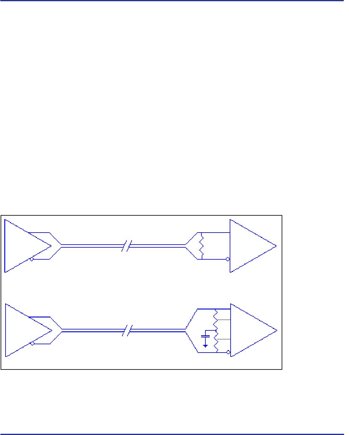
LVDS Driver Termination
For a general LVDS interface, the recommended value for the
termination impedance (Z
T
) is between 90 and 132. The actual
value should be selected to match the differential impedance (Z
0
) of
your transmission line. A typical point-to-point LVDS design uses a
100 parallel resistor at the receiver and a 100 differential
transmission-line environment. In order to avoid any
transmission-line reflection issues, the components should be
surface mounted and must be placed as close to the receiver as
possible. IDT offers a full line of LVDS compliant devices with two
types of output structures: current source and voltage source. The
standard termination schematic as shown in Figure 1A can be used
with either type of output structure. Figure 1B, which can also be
used with both output types, is an optional termination with center tap
capacitance to help filter common mode noise. The capacitor value
should be approximately 50pF. If using a non-standard termination, it
is recommended to contact IDT and confirm if the output structure is
current source or voltage source type. In addition, since these
outputs are LVDS compatible, the input receiver’s amplitude and
common-mode input range should be verified for compatibility with
the output.
LVDS Termination
LVDS
Driver
LVDS
Driver
LVDS
Receiver
LVDS
Receiver
Z
T
C
Z
O
• Z
T
Z
O
• Z
T
Z
T
2
Z
T
2
Figure 1A. Standard Termination
Figure 1B. Optional Termination