IDT8N4Q001 REV G Data Sheet QUAD-FREQUENCY PROGRAMMABLE-XO
IDT8N4Q001GCD REVISION A
MARCH 6, 2012
7 ©2012 Integrated Device Technology, Inc.
AC Electrical Characteristics
Table 6. AC Characteristics, V
DD
= 3.3V ± 5% or 2.5V ± 5%, T
A
= -40°C to 85°C
Symbol Parameter Test Conditions Minimum Typical Maximum Units
f
OUT
Output Frequency Q, nQ
Output Divider, N = 3 to126 15.476 866.67 MHz
Output Divider, N = 2 975 1,300 MHz
f
I
Initial Accuracy Measured at 25°C ±10 ppm
f
S
Temperature Stability
Option code = A or B ±100 ppm
Option code = E or F ±50 ppm
Option code = K or L ±20 ppm
f
A
Aging
Frequency drift over 10 year life ±3 ppm
Frequency drift over 15 year life ±5 ppm
f
T
Total Stability
Option code A or B (10 year life) ±113 ppm
Option code E or F (10 year life) ±63 ppm
Option code K or L (10 year life) ±33 ppm
tjit(cc) Cycle-to-Cycle Jitter; NOTE 1 20 ps
tjit(per) RMS Period Jitter; NOTE 1 2.85 4 ps
tjit(Ø)
RMS Phase Jitter (Random):
Fractional PLL feedback and
f
XTAL
=100.000MHz (2xxx order
codes)
17 MHz f
OUT
1300 MHz,
NOTE 2,3,4
0.440 0.995 ps
RMS Phase Jitter (Random);
Integer PLL feedback and
f
XTAL
=100.00MHz (1xxx order codes)
500 MHz f
OUT
1300 MHz,
NOTE 2,3,4
0.240 0.390 ps
125 MHz f
OUT
500 MHz,
NOTE 2,3,4
0.245 0.425 ps
17 MHz f
OUT
125 MHz,
NOTE 2,3,4
0.350 0.555 ps
f
OUT
156.25 MHz, NOTE 2, 3, 4 0.253 ps
f
OUT
156.25 MHz,NOTE 2, 3, 5 0.263 ps
RMS Phase Jitter (Random)
Fractional PLL feedback and
f
XTAL
=114.285MHz (0xxx order codes)
17 MHz f
OUT
1300 MHz,
NOTE 2, 3, 4
0.475 0.990 ps
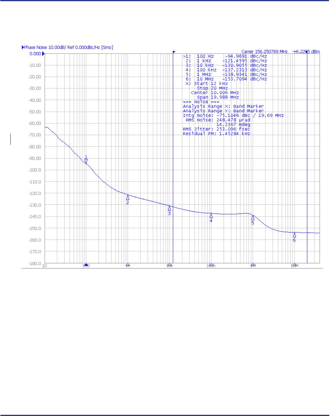
N
(100)
Single-side band phase noise,
100Hz from Carrier
156.25MHz -94.7 dBc/Hz
N
(1k)
Single-side band phase noise,
1kHz from Carrier
156.25MHz -121.5 dBc/Hz
N
(10k)
Single-side band phase noise,
10kHz from Carrier
156.25MHz -130.9 dBc/Hz
N
(100k)
Single-side band phase noise,
100kHz from Carrier
156.25MHz -137.2 dBc/Hz
N
(1M)
Single-side band phase noise,
1MHz from Carrier
156.25MHz -138.9 dBc/Hz
N
(10M)
Single-side band phase noise,
10MHz from Carrier
156.25MHz -153.7 dBc/Hz
PSNR Power Supply Noise Rejection
50mV Sinusoidal Noise
1kHz - 50kHz
-54 dB
t
R
/ t
F
Output Rise/Fall Time 20% to 80% 100 425 ps