MAX1240/MAX1241
+2.7V, Low-Power,
12-Bit Serial ADCs in 8-Pin SO
10 ______________________________________________________________________________________
Using
SHDN
to Reduce Supply Current
Power consumption can be reduced significantly by
shutting down the MAX1240/MAX1241 between con-
versions. Figure 6 shows a plot of average supply cur-
rent versus conversion rate. Because the MAX1241
uses an external reference voltage (assumed to be pre-
sent continuously), it “wakes up” from shutdown more
quickly (in 4µs) and therefore provides lower average
supply currents. The wake-up time (t
WAKE
) is the time
from when SHDN is deasserted to the time when a con-
version may be initiated (Figure 5). For the MAX1240,
this time depends on the time in shutdown (Figure 7)
because the external 4.7µF reference bypass capacitor
loses charge slowly during shutdown.
External Clock
The actual conversion does not require the external
clock. This allows the conversion result to be read back
at the µP’s convenience at any clock rate from up to
2.1MHz. The clock duty cycle is unrestricted if each
clock phase is at least 200ns. Do not run the clock
while a conversion is in progress.
Timing and Control
Conversion-start and data-read operations are controlled
by the
CS
and SCLK digital inputs. The timing diagrams
of Figures 8 and 9 outline serial-interface operation.
A
CS
falling edge initiates a conversion sequence: the
T/H stage holds the input voltage, the ADC begins to
convert, and DOUT changes from high impedance to
logic low. SCLK must be kept low during the conver-
sion. An internal register stores the data when the con-
version is in progress.
10
1
0.01
0.001
0.1 1 10 100 1k 10k 100k
0.1
CONVERSION RATE (Hz)
SUPPLY CURRNET (mA)
V
DD
=
V
REF
= 3.0V
R
LOAD
=
, C
LOAD
= 50pF
CODE = 010101010000
MAX1241 FIG. 06a
MAX1241
MAX1240
Figure 6. Average Supply Current vs. Conversion Rate
1.0
0.0
0.001 0.01 0.1 1 10
0.8
0.6
0.4
0.2
TIME IN SHUTDOWN
(sec)
POWER-UP DELAY (ms)
MAX1240/41-07a
Figure 7. Typical Reference Power-Up Delay vs. Time in
Shutdown
EOC
INTERFACE IDLE
CONVERSION
IN PROGRESS
EOC
0μs
TRAILING
ZEROS
IDLE
CLOCK OUT SERIAL DATA
TRACK/HOLD
STATE
TRACK
HOLD
TRACK
DOUT B11 B10 B9 B8 B7 B6 B5 B4 B3 B2 B1 B0
SCLK
14 8 12 16
7.5μs (t
CONV
)
HOLD
0μs
(t
CS
)
TOTAL = 13.7μs
12.5 × 0.476μs = 5.95μs
CYCLE TIME
CS
0.24
μ
s
Figure 8. Interface Timing Sequence
End of conversion (EOC) is signaled by DOUT going
high. DOUT’s rising edge can be used as a framing
signal. SCLK shifts the data out of this register any time
after the conversion is complete. DOUT transitions on
SCLK’s falling edge. The next falling clock edge pro-
duces the MSB of the conversion at DOUT, followed by
the remaining bits. Since there are 12 data bits and one
leading high bit, at least 13 falling clock edges are
needed to shift out these bits. Extra clock pulses occur-
ring after the conversion result has been clocked out,
and prior to a rising edge of
CS
, produce trailing zeros
at DOUT and have no effect on converter operation.
Minimum cycle time is accomplished by using DOUT’s
rising edge as the EOC signal. Clock out the data with
12.5 clock cycles at full speed. Pull
CS
high after reading
the conversion’s LSB. After the specified minimum time
(t
CS
),
CS
can be pulled low again to initiate the next
conversion.
Output Coding and Transfer Function
The data output from the MAX1240/MAX1241 is binary,
and Figure 10 depicts the nominal transfer function.
Code transitions occur halfway between successive-
integer LSB values. If V
REF
= +2.500V, then 1 LSB =
610µV or 2.500V/4096.
____________Applications Information
Connection to Standard Interfaces
The MAX1240/MAX1241 serial interface is fully compat-
ible with SPI/QSPI and MICROWIRE standard serial
interfaces (Figure 11).
If a serial interface is available, set the CPU’s serial
interface in master mode so the CPU generates the ser-
ial clock. Choose a clock frequency up to 2.1MHz.
1) Use a general-purpose I/O line on the CPU to pull
CS
low. Keep SCLK low.
2) Wait the for the maximum conversion time specified
before activating SCLK. Alternatively, look for a DOUT
rising edge to determine the end of conversion.
3) Activate SCLK for a minimum of 13 clock cycles. The
first falling clock edge produces the MSB of the
DOUT conversion. DOUT output data transitions on
SCLK’s falling edge and is available in MSB-first for-
mat. Observe the SCLK to DOUT valid timing char-
acteristic. Data can be clocked into the µP on
SCLK’s rising edge.
4) Pull
CS
high at or after the 13th falling clock edge. If
CS
remains low, trailing zeros are clocked out after
the LSB.
MAX1240/MAX1241
+2.7V, Low-Power,
12-Bit Serial ADCs in 8-Pin SO
______________________________________________________________________________________ 11
11
111
11
110
11
101
00
011
00
010
00
001
00000
012 FS
OUTPUT CODE
FS - 3/2 LSBINPUT VOLTAGE (LSBs)
FS = V
REF
- 1 LSB
1 LSB =
V
REF
4096
FULL-SCALE
TRANSITION
3
CS
SCLK
DOUT
INTERNAL
T/H
(TRACK/ACQUIRE)
t
CS0
t
CONV
t
DV
t
APR
t
STR
(HOLD) (TRACK/ACQUIRE)
B2 B1 B0
t
CH
t
DO
t
CL
t
TR
t
CS
Figure 10. Unipolar Transfer Function, Full Scale (FS) = V
REF
-
1 LSB, Zero Scale (ZS) = GND
Figure 9. Detailed Serial-Interface Timing
MAX1240/MAX1241
+2.7V, Low-Power,
12-Bit Serial ADCs in 8-Pin SO
12 ______________________________________________________________________________________
5) With CS = high, wait the minimum specified time, t
CS
,
before initiating a new conversion by pulling CS low.
If a conversion is aborted by pulling CS high before
the conversion’s end, wait for the minimum acquisi-
tion time, t
ACQ
, before starting a new conversion.
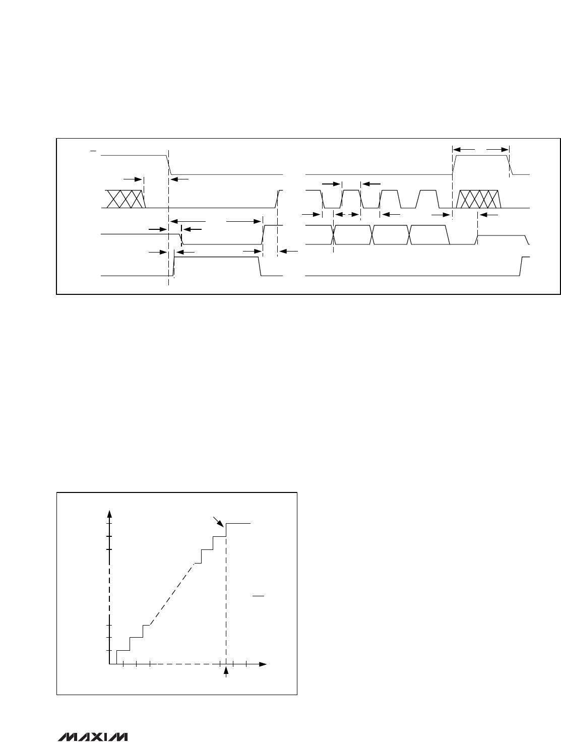
CS must be held low until all data bits are clocked out.
Data can be output in two bytes or continuously, as
shown in Figure 8. The bytes contain the result of the
conversion padded with one leading 1, and trailing 0s.
SPI and MICROWIRE
When using SPI or MICROWIRE, set CPOL = 0 and
CPHA = 0. Conversion begins with a
CS
falling edge.
DOUT goes low, indicating a conversion in progress. Wait
until DOUT goes high or until the maximum specified
7.5µs conversion time elapses. Two consecutive 1-byte
reads are required to get the full 12 bits from the ADC.
DOUT output data transitions on SCLK’s falling edge and
is clocked into the µP on SCLK’s rising edge.
The first byte contains a leading 1, and seven bits of con-
version result. The second byte contains the remaining
five bits and three trailing zeros. See Figure 11 for con-
nections and Figure 12 for timing.
QSPI
Set CPOL = CPHA = 0. Unlike SPI, which requires two
1-byte reads to acquire the 12 bits of data from the ADC,
QSPI allows the minimum number of clock cycles neces-
sary to clock in the data. The MAX1240/MAX1241
requires 13 clock cycles from the µP to clock out the 12
bits of data with no trailing zeros (Figure 13). The maxi-
mum clock frequency to ensure compatibility with QSPI is
2.097MHz.
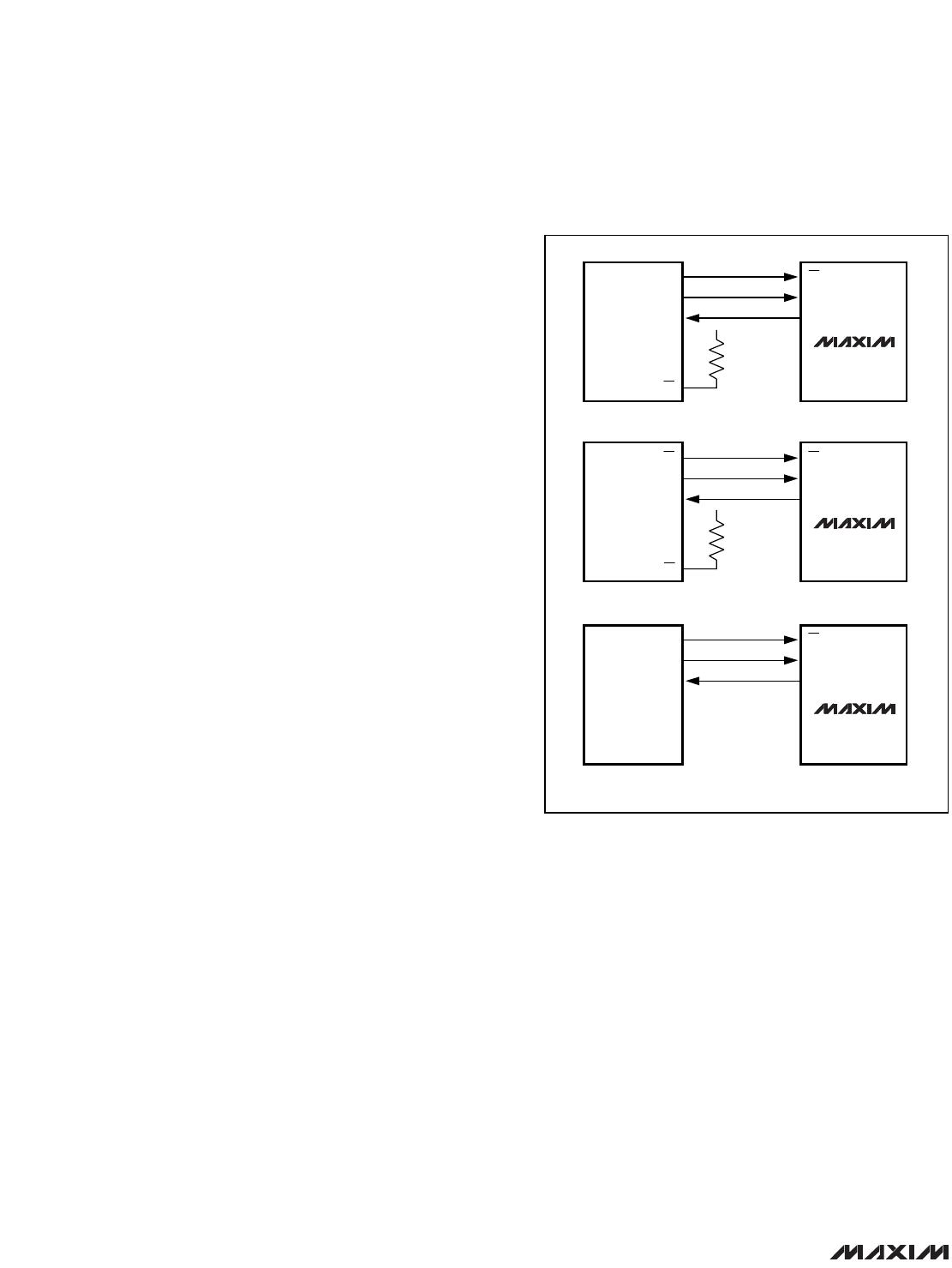
Layout, Grounding, and Bypassing
For best performance, use printed circuit boards. Wire-
wrap boards are not recommended. Board layout should
ensure that digital and analog signal lines are separated
from each other. Do not run analog and digital (especially
clock) lines parallel to one another, or digital lines under-
neath the ADC package.
Figure 14 shows the recommended system ground con-
nections. Establish a single-point analog ground (“star”
ground point) at GND, separate from the logic ground.
Connect all other analog grounds and DGND to this star
ground point for further noise reduction. No other digital
system ground should be connected to this single-point
analog ground. The ground return to the power supply for
this ground should be low impedance and as short as
possible for noise-free operation.
High-frequency noise in the V
DD
power supply may affect
the ADC’s high-speed comparator. Bypass this supply to
the single-point analog ground with 0.1µF and 4.7µF
bypass capacitors. Minimize capacitor lead lengths for
best supply-noise rejection. If the power supply is very
noisy, a 10Ω resistor can be connected as a lowpass filter
to attenuate supply noise (Figure 14).
CS
SCLK
DOUT
I/O
SCK
MISO
+3V
SS
a) SPI
CS
SCLK
DOUT
CS
SCK
MISO
+3V
SS
b) QSPI
MAX1240
MAX1241
MAX1240
MAX1241
MAX1240
MAX1241
CS
SCLK
DOUT
I/O
SK
SI
c) MICROWIRE
Figure 11. Common Serial-Interface Connections to the
MAX1241

MAX1240ACSA+T

Mfr. #:
Manufacturer:
Maxim Integrated
Description:
Analog to Digital Converters - ADC 12-Bit 73ksps 3.6V Precision ADC
Lifecycle:
New from this manufacturer.
Delivery:
DHL FedEx Ups TNT EMS
Payment:
T/T Paypal Visa MoneyGram Western Union