MAX1240/MAX1241
+2.7V, Low-Power,
12-Bit Serial ADCs in 8-Pin SO
_______________________________________________________________________________________ 7
_______________________________________________________________________Pin Description
6 DOUT
Serial Data Output. Data changes state at SCLK’s falling edge. DOUT is high impedance when CS is
high.
8 SCLK
3
SHDN
Three-Level Shutdown Input. Pulling SHDN low shuts the MAX1240/MAX1241 down to 15µA (max)
supply current. Both the MAX1240 and MAX1241 are fully operational with either SHDN high or
unconnected. For the MAX1240, pulling SHDN high enables the internal reference, and letting SHDN
open disables the internal reference and allows for the use of an external reference.
4 REF
Reference Voltage for Analog-to-Digital Conversion. Internal 2.5V reference output for MAX1240;
bypass with 4.7µF capacitor. External reference voltage input for MAX1241, or for MAX1240 with the
internal reference disabled. Bypass REF with a minimum of 0.1µF when using an external reference.
7
CS
Active-Low Chip Select initiates conversions on the falling edge. When CS is high, DOUT is high
impedance.
5 GND Analog and Digital Ground
2 AIN Sampling Analog Input, 0V to V
REF
range
NAME FUNCTION
1 V
DD
Positive Supply Voltage: 2.7V to 3.6V, (MAX1240); 2.7V to 5.25V (MAX1241)
PIN
Serial Clock Input. SCLK clocks data out at rates up to 2.1MHz.
0.6
INTEGRAL NONLINEARITY
vs. CODE
-0.6
0
-0.2
-0.4
0.4
0.2
MAX1241-11A/NEW
INL (LSB)
CODE
1024 2048 3072
40960
20
-140
0
37.50
FFT PLOT
-120
0
-80
-100
-40
-20
-60
18.75
AMPLITUDE (dB)
FREQUENCY (kHz)
f
AIN
= 10kHz, 2.5V
P-P
f
SAMPLE
= 73ksps
MAX1241-TOC12A
____________________________Typical Operating Characteristics (continued)
(V
DD
= 3.0V, REF = 2.5V, f
SCLK
= 2.1MHz, C
L
= 20pF, T
A
= +25°C, unless otherwise noted.)
MAX1240/MAX1241
+2.7V, Low-Power,
12-Bit Serial ADCs in 8-Pin SO
8 _______________________________________________________________________________________
_______________Detailed Description
Converter Operation
The MAX1240/MAX1241 use an input track/hold (T/H)
and successive-approximation register (SAR) circuitry
to convert an analog input signal to a digital 12-bit out-
put. No external-hold capacitor is needed for the T/H.
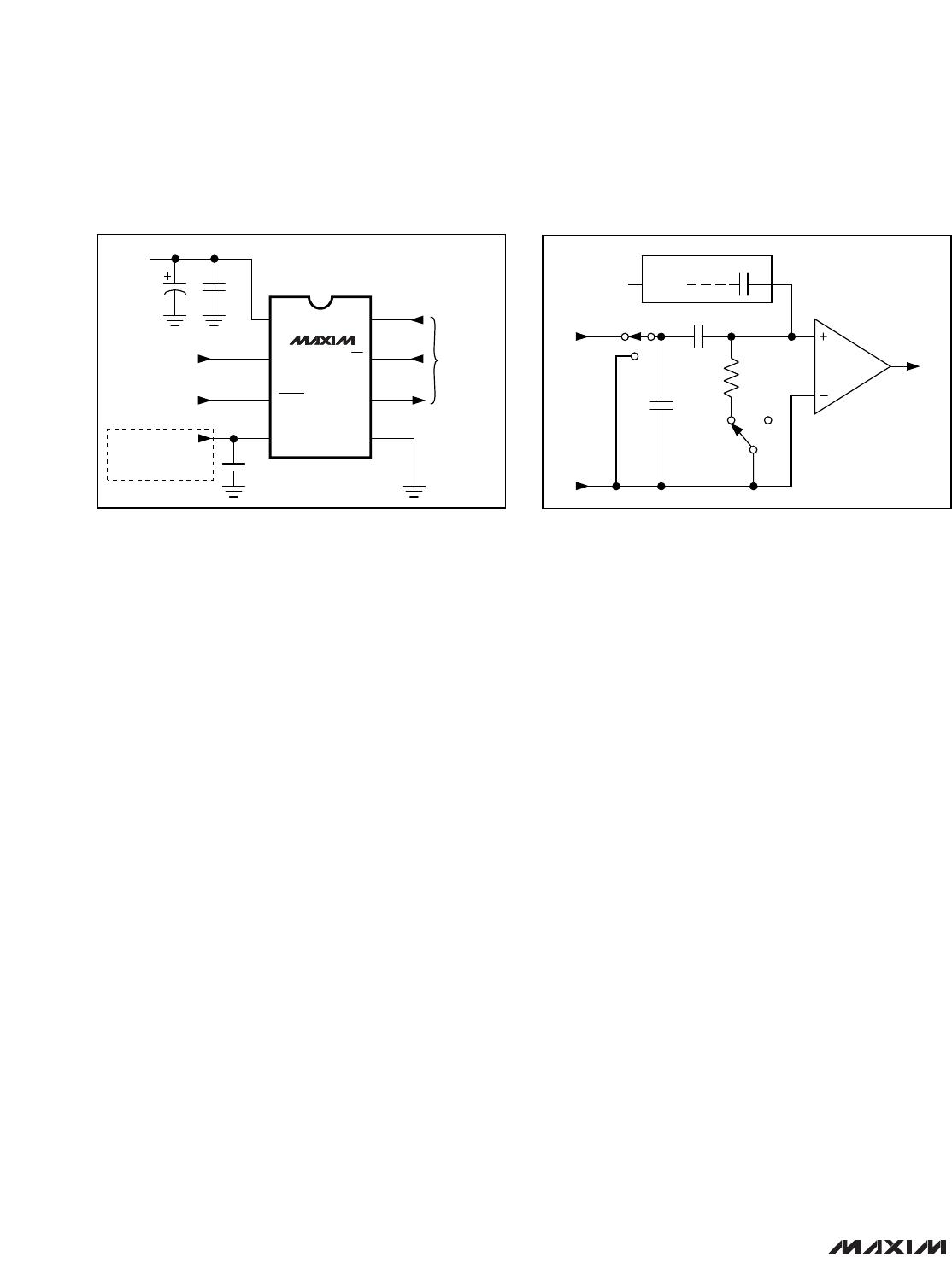
Figure 3 shows the MAX1240/MAX1241 in its simplest
configuration. The MAX1240/MAX1241 convert input
signals in the 0V to V
REF
range in 9µs, including T/H
acquisition time. The MAX1240’s internal reference is
trimmed to 2.5V, while the MAX1241 requires an external
reference. Both devices accept voltages from 1.0V to
V
DD
. The serial interface requires only three digital lines
(SCLK,
CS,
and DOUT) and provides an easy interface
to microprocessors (µPs).
The MAX1240/MAX1241 have two modes: normal and
shutdown. Pulling
SHDN
low shuts the device down and
reduces supply current below 10µA (V
DD
3.6V
), while
pulling
SHDN
high or leaving it open puts the device
into operational mode. Pulling CS low initiates a conver-
sion. The conversion result is available at DOUT in
unipolar serial format. The serial data stream consists
of a high bit, signaling the end of conversion (EOC), fol-
lowed by the data bits (MSB first).
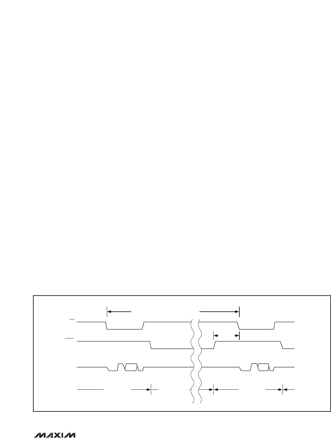
Analog Input
Figure 4 illustrates the sampling architecture of the ana-
log-to-digital converter’s (ADC’s) comparator. The full-
scale input voltage is set by the voltage at REF.
Track/Hold
In track mode, the analog signal is acquired and stored
in the internal hold capacitor. In hold mode, the T/H
switch opens and maintains a constant input to the
ADC’s SAR section.
During acquisition, the analog input (AIN) charges
capacitor C
HOLD
. Bringing
CS
low ends the acquisition
interval. At this instant, the T/H switches the input side
of C
HOLD
to GND. The retained charge on C
HOLD
repre-
sents a sample of the input, unbalancing node ZERO at
the comparator’s input.
In hold mode, the capacitive digital-to-analog converter
(DAC) adjusts during the remainder of the conversion
cycle to restore node ZERO to 0V within the limits of 12-
bit resolution. This action is equivalent to transferring a
charge from C
HOLD
to the binary-weighted capacitive
DAC, which in turn forms a digital representation of the
analog input signal. At the conversion’s end, the input
side of C
HOLD
switches back to AIN, and C
HOLD
charges to the input signal again.
The time required for the T/H to acquire an input signal
is a function of how quickly its input capacitance is
charged. If the input signal’s source impedance is high,
the acquisition time lengthens and more time must be
allowed between conversions. The acquisition time
(t
ACQ
) is the maximum time the device takes to acquire
the signal, and is also the minimum time needed for the
signal to be acquired. Acquisition time is calculated by:
t
ACQ
= 9(R
S
+ R
IN
) x 16pF
where R
IN
= 9kΩ, R
S
= the input signal’s source imped-
ance, and t
ACQ
is never less than 1.5µs. Source imped-
ances below 1kΩ do not significantly affect the ADC’s
AC performance.
Higher source impedances can be used if a 0.01µF
capacitor is connected to the analog input. Note that
the input capacitor forms an RC filter with the input
source impedance, limiting the ADC’s input signal
bandwidth.
AIN
TRACK
INPUT
HOLD
GND
TRACK
HOLD
9k
R
IN
C
HOLD
16pF
-+
C
SWITCH
COMPARATOR
ZERO
REF
12-BIT CAPACITIVE DAC
AT THE SAMPLING INSTANT,
THE INPUT SWITCHES FROM
AIN TO GND.
SHUTDOWN
INPUT
ANALOG INPUT
0V TO V
REF
+2.7V to +3.6V* *
**
V
DD,MAX
= +5.25V (MAX1241)
4.7μF (MAX1240)
0.1μF (MAX1241)
1
2
3
4
V
DD
AIN
SHDN
REF
8
7
6
5
SCLK
CS
DOUT
GND
SERIAL
INTERFACE
C**
4.7μF 0.1μF
REFERENCE
INPUT
(MAX1241 ONLY)
MAX1240
MAX1241
Figure 3. Operational Diagram
Figure 4. Equivalent Input Circuit
MAX1240/MAX1241
+2.7V, Low-Power,
12-Bit Serial ADCs in 8-Pin SO
_______________________________________________________________________________________ 9
Input Bandwidth
The ADCs’ input tracking circuitry has a 2.25MHz small-
signal bandwidth, so it is possible to digitize high-
speed transient events and measure periodic signals
with bandwidths exceeding the ADC’s sampling rate by
using undersampling techniques. To avoid aliasing of
unwanted high-frequency signals into the frequency
band of interest, anti-alias filtering is recommended.
Analog Input Protection
Internal protection diodes, which clamp the analog
input to V
DD
and GND, allow the input to swing from
GND - 0.3V to V
DD
+ 0.3V without damage. However,
for accurate conversions near full scale, the input must
not exceed V
DD
by more than 50mV, or be lower than
GND by 50mV.
If the analog input exceeds 50mV beyond the sup-
plies, limit the input current to 2mA.
Internal Reference (MAX1240)
The MAX1240 has an on-chip voltage reference
trimmed to 2.5V. The internal reference output is con-
nected to REF and also drives the internal capacitive
DAC. The output can be used as a reference voltage
source for other components and can source up to
400µA. Bypass REF with a 4.7µF capacitor. Larger
capacitors increase wake-up time when exiting shut-
down (see the section Using
SHDN
to Reduce Supply
Current). The internal reference is enabled by pulling the
SHDN pin high. Letting SHDN open disables the internal
reference, which allows the use of an external reference,
as described in the External Reference section.
External Reference
The MAX1240/MAX1241 operate with an external refer-
ence at the REF pin. To use the MAX1240 with an
external reference, disable the internal reference by let-
ting SHDN open. Stay within the +1.0V to V
DD
voltage
range to achieve specified accuracy. The minimum
input impedance is 18kΩ for DC currents. During con-
version, the external reference must be able to deliver
up to 250µA of DC load current and have an output
impedance of 10Ω or less. The recommended mini-
mum value for the bypass capacitor is 0.1µF. If the ref-
erence has higher output impedance or is noisy,
bypass it close to the REF pin with a 4.7µF capacitor.
____________________Serial Interface
Initialization after Power-Up and
Starting a Conversion
When power is first applied, and if SHDN is not pulled
low, it takes the fully discharged 4.7µF reference
bypass capacitor up to 20ms to provide adequate
charge for specified accuracy. With an external refer-
ence, the internal reset time is 10µs after the power
supplies have stabilized. No conversions should be
performed during these times.
To start a conversion, pull
CS
low. At
CS’s
falling edge,
the T/H enters its hold mode and a conversion is initiat-
ed. After an internally timed conversion period, the end
of conversion is signaled by DOUT pulling high. Data
can then be shifted out serially with the external clock.
COMPLETE CONVERSION SEQUENCE
t
WAKE
POWERED UPPOWERED DOWNPOWERED UP
CONVERSION 0 CONVERSION 1
DOUT
CS
SHDN
Figure 5. Shutdown Sequence

MAX1240ACSA+T

Mfr. #:
Manufacturer:
Maxim Integrated
Description:
Analog to Digital Converters - ADC 12-Bit 73ksps 3.6V Precision ADC
Lifecycle:
New from this manufacturer.
Delivery:
DHL FedEx Ups TNT EMS
Payment:
T/T Paypal Visa MoneyGram Western Union