V
DD
= 3.6V
MAX1240/MAX1241
+2.7V, Low-Power,
12-Bit Serial ADCs in 8-Pin SO
4 _______________________________________________________________________________________
ELECTRICAL CHARACTERISTICS (continued)
(V
DD
= +2.7V to +3.6V (MAX1240); V
DD
= +2.7V to +5.25V (MAX1241); 73ksps, f
S
CLK
= 2.1MHz (50% duty cycle); MAX1240—4.7µF
capacitor at REF pin, MAX1241—external reference; V
REF
= 2.500V applied to REF pin; T
A
= T
MIN
to T
MAX
; unless otherwise noted.)
Note 1: Tested at V
DD
= +2.7V.
Note 2: Relative accuracy is the deviation of the analog value at any code from its theoretical value after the full-scale range and
offset have been calibrated.
Note 3: MAX1240—internal reference, offset nulled; MAX1241—external reference (V
REF
= +2.500V), offset nulled.
Note 4: External load should not change during conversion for specified accuracy.
Note 5: Guaranteed by design. Not subject to production testing.
Note 6: Measured as [V
FS
(2.7V) - V
FS
(V
DD(MAX
)].
Note 7: To guarantee acquisition time, t
ACQ
is the maximum time the device takes to acquire the signal, and is also the minimum
time needed for the signal to be acquired.
SCLK Pulse Width Low t
CL
200 ns
SCLK Pulse Width High t
CH
200 ns
SCLK Clock Frequency f
SCLK
0 2.1 MHz
CS Rise to Output Disable
t
TR
240 ns
SCLK Low to CS Fall Setup Time
t
CS0
50 ns
DOUT Rise to SCLK Rise (Note 5) t
STR
0 ns
CS Pulse Width
t
CS
240 ns
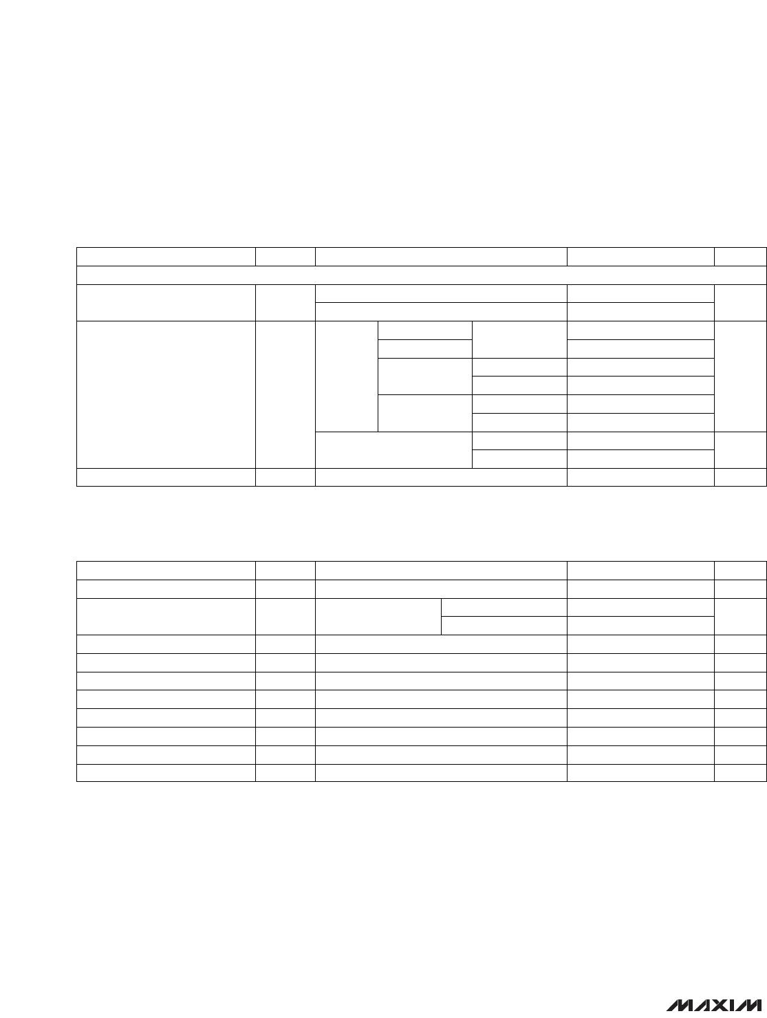
Figure 2, C
LOAD
= 50pF
CS Fall to Output Enable
t
DV
240 nsFigure 1, C
LOAD
= 50pF
PARAMETERS SYMBOL MIN TYP MAX UNITSCONDITIONS
Acquisition Time t
ACQ
1.5 µs
CS = V
DD
(Note 6)
TIMING CHARACTERISTICS (Figure 8)
(V
DD
= +2.7V to +3.6V (MAX1240); V
DD
= +2.7V to +5.25V (MAX1241); T
A
= T
MIN
to T
MAX
, unless otherwise noted.)
PARAMETERS SYMBOL MIN TYP MAX UNITSCONDITIONS
2.7 3.6MAX1240
2.7 5.25MAX1241
V
DD
Supply Voltage V
±0.3(Note 5)PSRSupply Rejection mV
20 240
SCLK Fall to Output Data Valid t
DO
20 200
ns
Figure 1,
C
LOAD
= 50pF
MAX124_ _C/E
MAX124_ _M
1.4 2.0
Operating
mode
1.6 2.5
V
DD
= 3.6V
3.5 15
V
DD
= 5.25V
V
DD
= 3.6V
V
DD
= 5.25V
I
DD
1.9 10
Power-down, digital inputs
at 0V or V
DD
1.4 3.5
µA
0.9 1.5
V
DD
= 3.6V
MAX1240C
MAX1241A/B
Supply Current
MAX1240A/B
mA
1.6 3.8
V
DD
= 3.6V
V
DD
= 5.25V
0.9 2.8
MAX1241C
POWER REQUIREMENTS