REV. C
a
Information furnished by Analog Devices is believed to be accurate and
reliable. However, no responsibility is assumed by Analog Devices for its
use, nor for any infringements of patents or other rights of third parties that
may result from its use. No license is granted by implication or otherwise
under any patent or patent rights of Analog Devices.
One Technology Way, P.O. Box 9106, Norwood, MA 02062-9106, U.S.A.
Tel: 781/329-4700www.analog.com
Fax: 781/326-8703 © Analog Devices, Inc., 2002
AD828
Dual, Low Power
Video Op Amp
FEATURES
Excellent Video Performance
Differential Gain and Phase Error of 0.01% and 0.05
High Speed
130 MHz 3 dB Bandwidth (G = +2)
450 V/s Slew Rate
80 ns Settling Time to 0.01%
Low Power
15 mA Max Power Supply Current
High Output Drive Capability
50 mA Minimum Output Current per Amplifier
Ideal for Driving Back Terminated Cables
Flexible Power Supply
Specified for +5 V, 5 V, and 15 V Operation
3.2 V Min Output Swing into a 150 Load
(V
S
= 5 V)
Excellent DC Performance
2.0 mV Input Offset Voltage
Available in 8-Lead SOIC and 8-Lead Plastic Mini-DIP
FUNCTIONAL BLOCK DIAGRAM
1
2
3
4
8
7
6
5
AD828
V+
OUT2
–IN2
+IN2
OUT1
–IN1
+IN1
V–
GENERAL DESCRIPTION
The AD828 is a low cost, dual video op amp optimized for use
in video applications that require gains of +2 or greater and
high output drive capability, such as cable driving. Due to its
low power and single-supply functionality, along with excellent
differential gain and phase errors, the AD828 is ideal for power-
sensitive applications such as video cameras and professional
video equipment.
With video specs like 0.1 dB flatness to 40 MHz and low
differential gain and phase errors of 0.01% and 0.05°, along
with 50 mA of output current per amplifier, the AD828 is an
excellent choice for any video application. The 130 MHz gain
bandwidth and 450 V/µs slew rate make the AD828 useful in
many high speed applications, including video monitors, CATV,
color copiers, image scanners, and fax machines.
1/2
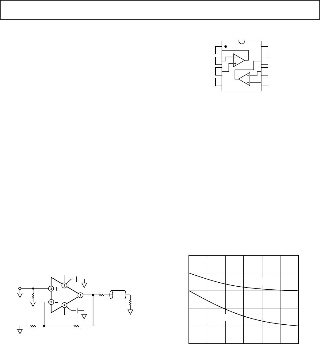
AD828
0.1F
0.1F
+V
–V
R
BT
75
75
R
T
75
1k
R
T
75
1k
V
IN
Figure 1. Video Line Driver
The AD828 is fully specified for operation with a single 5 V
power supply and with dual supplies from ±5 V to ±15 V. This
power supply flexibility, coupled with a very low supply current
of 15 mA and excellent ac characteristics under all power supply
conditions, make the AD828 the ideal choice for many demand-
ing yet power-sensitive applications.
The AD828 is a voltage feedback op amp that excels as a gain
stage (gains > +2) or active filter in high speed and video systems
and achieves a settling time of 45 ns to 0.1%, with a low input
offset voltage of 2 mV max.
The AD828 is available in low cost, small 8-lead plastic mini-DIP
and SOIC packages.
0.04
15
0.07
0.05
0.06
510
0.03
0.01
0.02
SUPPLY VOLTAGE – V
DIFFERENTIAL PHASE – Degrees
DIFFERENTIAL GAIN – Percent
DIFF GAIN
DIFF PHASE
Figure 2. Differential Phase vs. Supply Voltage