Parameter Conditions V
S
Min Typ Max Unit
OUTPUT CHARACTERISTICS
Output Voltage Swing R
LOAD
= 500 Ω±5 V 3.3 3.8 ± V
R
LOAD
= 150 Ω±5 V 3.2 3.6 ± V
R
LOAD
= 1 kΩ±15 V 13.3 13.7 ±V
R
LOAD
= 500 Ω±15 V 12.8 13.4 ±V
1.5
R
LOAD
= 500 Ω 0, +5 V 3.5 ±V
Output Current ±15 V 50 mA
±5 V 40 mA
0, +5 V 30 mA
Short Circuit Current ±15 V 90 mA
Output Resistance Open-Loop 8 Ω
MATCHING CHARACTERISTICS
Dynamic
Crosstalk f = 5 MHz ±15 V –80 dB
Gain Flatness Match G = +1, f = 40 MHz ±15 V 0.2 dB
Skew Rate Match G = –1 ±15 V 10 V/µs
DC
Input Offset Voltage Match T
MIN
to T
MAX
±5 V, ±15 V 0.5 2 mV
Input Bias Current Match T
MIN
to T
MAX
±5 V, ±15 V 0.06 0.8 µA
Open-Loop Gain Match V
O
= ±10 V, R
L
= 1 kΩ, T
MIN
to T
MAX
±15 V 0.01 0.15 mV/V
Common-Mode Rejection Ratio Match V
CM
= ±12 V, T
MIN
to T
MAX
±15 V 80 100 dB
Power Supply Rejection Ratio Match ±5 V to ±15 V, T
MIN
to T
MAX
80 100 dB
POWER SUPPLY
Operating Range Dual Supply ±2.5 ± 18 V
Single Supply +5 +36 V
Quiescent Current ±5 V 14.0 15 mA
T
MIN
to T
MAX
±5 V 14.0 15 mA
T
MIN
to T
MAX
±5 V 15 mA
Power Supply Rejection Ratio V
S
= ±5 V to ±15 V, T
MIN
to T
MAX
80 90 dB
*Full power bandwidth = slew rate/2 π V
PEAK
.
Specifications subject to change without notice.
ABSOLUTE MAXIMUM RATINGS
1
Supply Voltage . . . . . . . . . . . . . . . . . . . . . . . . . . . . . . . . ±18 V
Internal Power Dissipation
2
Plastic DIP (N) . . . . . . . . . . . . . . . . . . See Derating Curves
Small Outline (R) . . . . . . . . . . . . . . . . . See Derating Curves
Input Voltage (Common Mode) . . . . . . . . . . . . . . . . . . . . ±V
S
Differential Input Voltage . . . . . . . . . . . . . . . . . . . . . . . . ±6 V
Output Short Circuit Duration . . . . . . . . See Derating Curves
Storage Temperature Range (N, R) . . . . . . . . –65°C to +125°C
Operating Temperature Range . . . . . . . . . . . . –40°C to +85°C
Lead Temperature Range (Soldering 10 sec) . . . . . . . . +300°C
NOTES
1
Stresses above those listed under Absolute Maximum Ratings may cause perma-
nent damage to the device. This is a stress rating only; functional operation of the
device at these or any other conditions above those indicated in the operational
section of this specification is not implied. Exposure to absolute maximum rating
conditions for extended periods may affect device reliability.
2
Specification is for device in free air:
8-Lead Plastic DIP Package: θ
JA
= 100°C/W
8-Lead SOIC Package: θ
JA
= 155°C/W
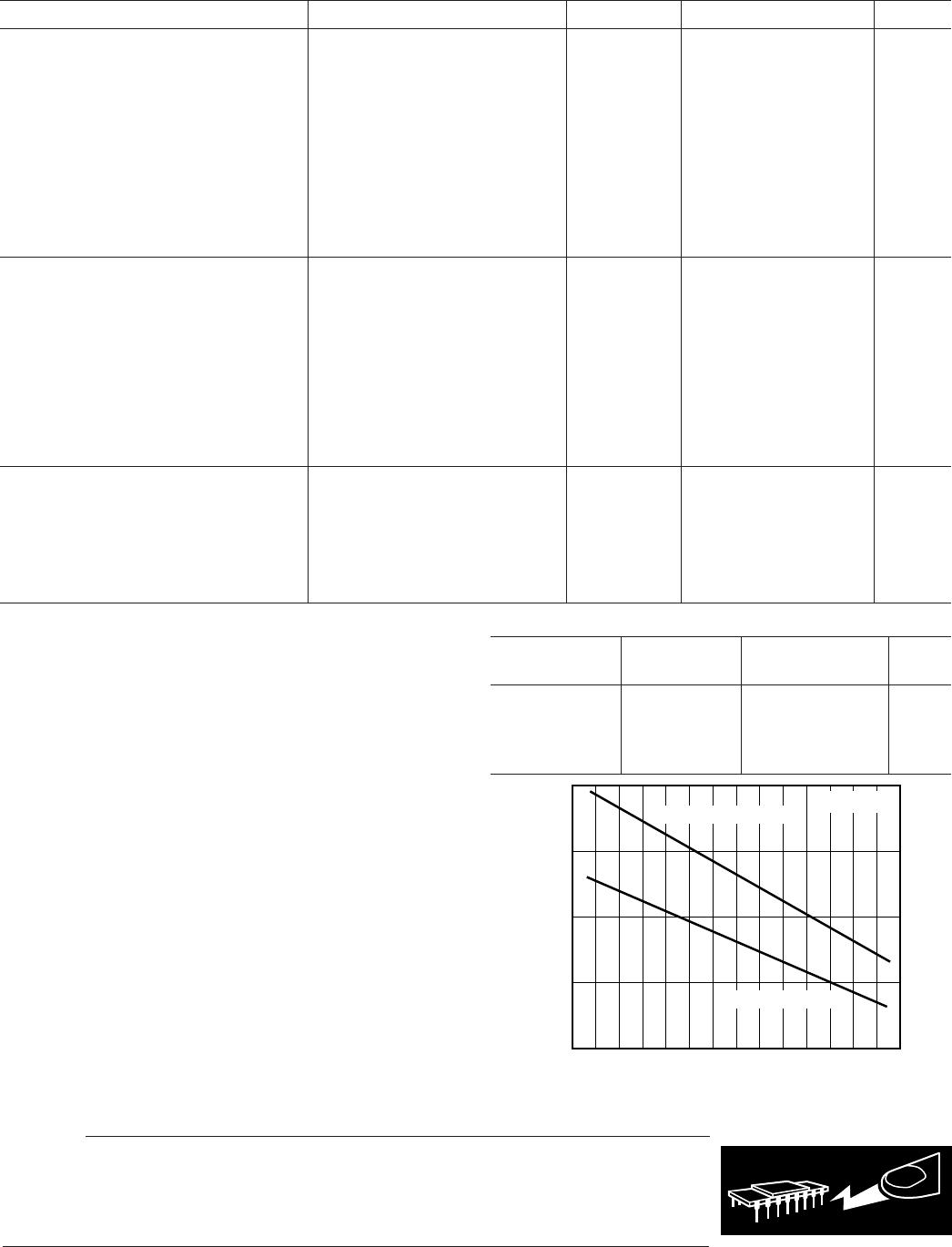
2.0
0
–50 90
1.5
0.5
–30
1.0
50 703010–10 80–40 40 60200–20
AMBIENT TEMPERATURE – C
MAXIMUM POWER DISSIPATION – Watts
8-LEAD MINI-DIP PACKAGE
8-LEAD SOIC PACKAGE
T
J
= 150C
Figure 3. Maximum Power Dissipation vs.
Temperature for Different Package Types
CAUTION
ESD (electrostatic discharge) sensitive device. Electrostatic charges as high as 4000 V readily
accumulate on the human body and test equipment and can discharge without detection. Although
the AD828 features proprietary ESD protection circuitry, permanent damage may occur on devices
subjected to high energy electrostatic discharges. Therefore, proper ESD precautions are
recommended to avoid performance degradation or loss of functionality.
WARNING!
ESD SENSITIVE DEVICE
REV. C
AD828
–3–
ORDERING GUIDE
Temperature Package Package
Model Range Description Option
AD828AN –40°C to +85°C 8-Lead Plastic DIP N-8
AD828AR –40°C to +85°C 8-Lead Plastic SOIC SO-8
AD828AR-REEL7 –40°C to +85°C 7" Tape and Reel SO-8
AD828AR-REEL –40°C to +85°C 13" Tape and Reel SO-8

