REV. C–10–
AD828
THEORY OF OPERATION
The AD828 is a low cost, dual video operational amplifier
designed to excel in high performance, high output current
video applications.
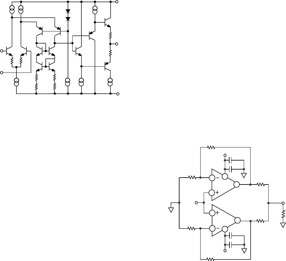
The AD828 consists of a degenerated NPN differential pair
driving matched PNPs in a folded-cascade gain stage (Figure 4).
The output buffer stage employs emitter followers in a class AB
amplifier that delivers the necessary current to the load while
maintaining low levels of distortion.
The AD828 will drive terminated cables and capacitive loads of
10 pF or less. As the closed-loop gain is increased, the AD828
will drive heavier cap loads without oscillating.
–IN
+IN
OUTPUT
+V
S
–V
S
Figure 4. Simplified Schematic
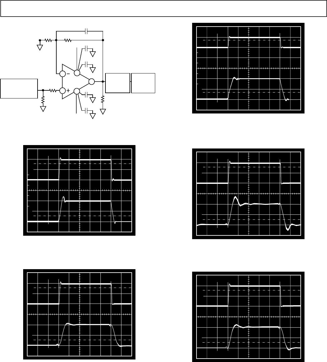
INPUT CONSIDERATIONS
An input protection resistor (R
IN
in TPC 31) is required in circuits
where the input to the AD828 will be subjected to transient or
continuous overload voltages exceeding the ±6 V maximum dif-
ferential limit. This resistor provides protection for the input
transistors by limiting their maximum base current.
For high performance circuits, the “balancing” resistor should be
used to reduce the offset errors caused by bias current flowing
through the input and feedback resistors. The balancing resistor
equals the parallel combination of R
IN
and R
F
and thus provides
a matched impedance at each input terminal. The offset voltage
error will then be reduced by more than an order of magnitude.
APPLYING THE AD828
The AD828 is a breakthrough dual amp that delivers precision and
speed at low cost with low power consumption. The AD828 offers
excellent static and dynamic matching characteristics, combined
with the ability to drive heavy resistive loads.
As with all high frequency circuits, care should be taken to main-
tain overall device performance as well as their matching. The
following items are presented as general design considerations.
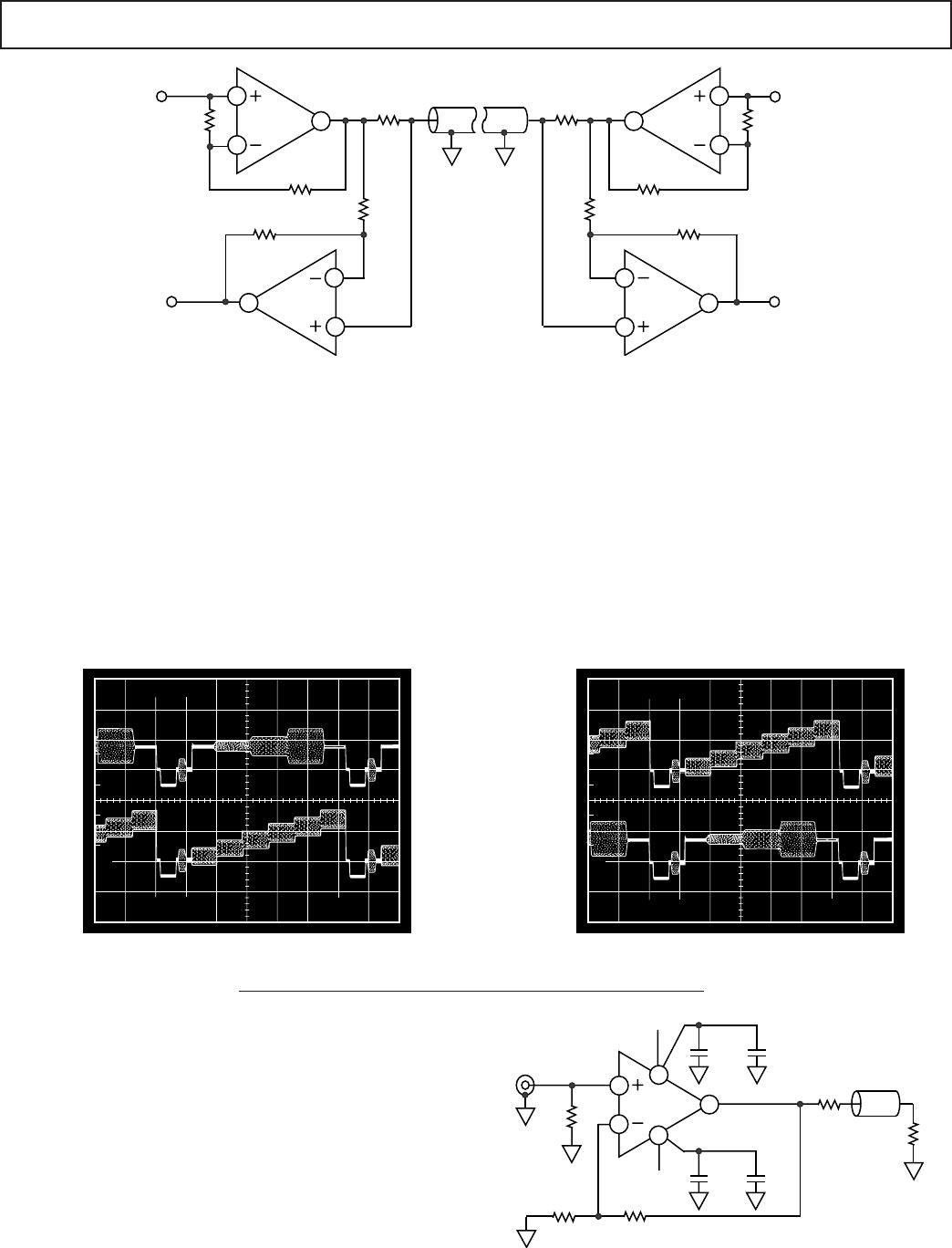
Circuit Board Layout
Input and output runs should be laid out so as to physically
isolate them from remaining runs. In addition, the feedback
resistor of each amplifier should be placed away from the feed-
back resistor of the other amplifier, since this greatly reduces
interamp coupling.
Choosing Feedback and Gain Resistors
To prevent the stray capacitance present at each amplifier’s
summing junction from limiting its performance, the feedback
resistors should be ≤ 1 kΩ. Since the summing junction capaci-
tance may cause peaking, a small capacitor (1 pF to 5 pF) may
be paralleled with R
F
to neutralize this effect. Finally, sockets
should be avoided, because of their tendency to increase interlead
capacitance.
Power Supply Bypassing
Proper power supply decoupling is critical to preserve the
integrity of high frequency signals. In carefully laid out designs,
decoupling capacitors should be placed in close proximity to
the supply pins, while their lead lengths should be kept to a
minimum. These measures greatly reduce undesired inductive
effects on the amplifier’s response.
Though two 0.1 µF capacitors will typically be effective in
decoupling the supplies, several capacitors of different values
can be paralleled to cover a wider frequency range.
PARALLEL AMPS PROVIDE 100 mA TO LOAD
By taking advantage of the superior matching characteristics of the
AD828, enhanced performance can easily be achieved by employ-
ing the circuit in Figure 5. Here, two identical cells are paralleled
to obtain even higher load driving capability than that of a single
amplifier (100 mA min guaranteed). R1 and R2 are included to
limit current flow between amplifier outputs that would arise in
the presence of any residual mismatch.
2
+V
S
V
IN
V
OUT
3
8
1k
R2
5
–V
S
R
L
1/2
AD828
1/2
AD828
1F
0.1F
7
5
6
1
1F
0.1F
4
R1
5
1k
1k
1k
Figure 5. Parallel Amp Configuration