MP1584 – 3A, 1.5MHz, 28V STEP-DOWN CONVERTER
MP1584 Rev. 1.0 www.MonolithicPower.com 8
8/8/2011 MPS Proprietary Information. Unauthorized Photocopy and Duplication Prohibited.
© 2011 MPS. All Rights Reserved.
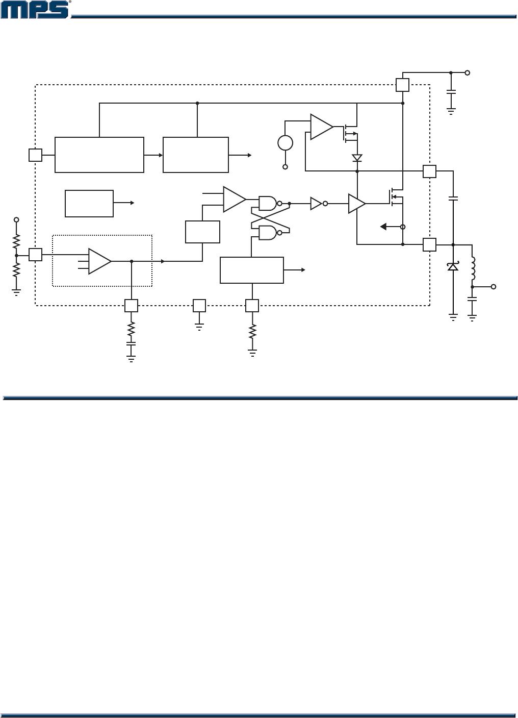
Error Amplifier
The error amplifier compares the FB pin voltage
with the internal reference (REF) and outputs a
current proportional to the difference between
the two. This output current is then used to
charge the external compensation network to
form the COMP voltage, which is used to
control the power MOSFET current.
During operation, the minimum COMP voltage
is clamped to 0.9V and its maximum is clamped
to 2.0V. COMP is internally pulled down to GND
in shutdown mode. COMP should not be pulled
up beyond 2.6V.
Internal Regulator
Most of the internal circuitries are powered from
the 2.6V internal regulator. This regulator takes
the VIN input and operates in the full VIN range.
When VIN is greater than 3.0V, the output of
the regulator is in full regulation. When VIN is
lower than 3.0V, the output decreases.
Enable Control
The MP1584 has a dedicated enable control pin
(EN). With high enough input voltage, the chip
can be enabled and disabled by EN which has
positive logic. Its falling threshold is a precision
1.2V, and its rising threshold is 1.5V (300mV
higher).
When floating, EN is pulled up to about 3.0V by
an internal 1µA current source so it is enabled.
To pull it down, 1µA current capability is
needed.
When EN is pulled down below 1.2V, the chip is
put into the lowest shutdown current mode.
When EN is higher than zero but lower than its
rising threshold, the chip is still in shutdown
mode but the shutdown current increases
slightly.
Under-Voltage Lockout (UVLO)
Under-voltage lockout (UVLO) is implemented
to protect the chip from operating at insufficient
supply voltage. The UVLO rising threshold is
about 3.0V while its falling threshold is a
consistent 2.6V.
Internal Soft-Start
The soft-start is implemented to prevent the
converter output voltage from overshooting
during startup. When the chip starts, the
internal circuitry generates a soft-start voltage
(SS) ramping up from 0V to 2.6V. When it is
lower than the internal reference (REF), SS
overrides REF so the error amplifier uses SS as
the reference. When SS is higher than REF,
REF regains control.
Thermal Shutdown
Thermal shutdown is implemented to prevent
the chip from operating at exceedingly high
temperatures. When the silicon die temperature
is higher than its upper threshold, it shuts down
the whole chip. When the temperature is lower
than its lower threshold, the chip is enabled
again.
Floating Driver and Bootstrap Charging
The floating power MOSFET driver is powered
by an external bootstrap capacitor. This floating
driver has its own UVLO protection. This
UVLO’s rising threshold is 2.2V with a threshold
of 150mV.
The bootstrap capacitor is charged and
regulated to about 5V by the dedicated internal
bootstrap regulator. When the voltage between
the BST and SW nodes is lower than its
regulation, a PMOS pass transistor connected
from VIN to BST is turned on. The charging
current path is from VIN, BST and then to SW.
External circuit should provide enough voltage
headroom to facilitate the charging.
As long as VIN is sufficiently higher than SW,
the bootstrap capacitor can be charged. When
the power MOSFET is ON, VIN is about equal
to SW so the bootstrap capacitor cannot be
charged. When the external diode is on, the
difference between VIN and SW is largest, thus
making it the best period to charge. When there
is no current in the inductor, SW equals the
output voltage V
OUT
so the difference between
V
IN
and V
OUT
can be used to charge the
bootstrap capacitor.