Expand menu
Hello, Sign in
My Account
0
Cart
Home
Products
Sensors
Semiconductors
Passive Components
Connectors
Power
Electromechanical
Optoelectronics
Circuit Protection
Integrated Circuits - ICs
Main Products
Manufacturers
Blog
Services
About OMO
About Us
Contact Us
Check Stock
STP80NF10FP
P1-P3
P4-P6
P7-P9
P10-P12
STP80
NF10FP
Electrical characteri
stics
7/12
Figure
7.
Gate cha
rge vs gate-source volt
age
Figure 8.
Ca
p
acit
ance variati
ons
Figure
9.
Norma
lized gate thresho
ld volt
age
vs tempera
ture
Figure 10.
Norm
alized on resistance vs
temp
erature
Fi
gu
re 1
1.
S
ou
rc
e-
dr
ain di
od
e fo
r
war
d
characteristics
Test c
ircui
t
ST
P80NF10F
P
8/12
3 T
est
circuit
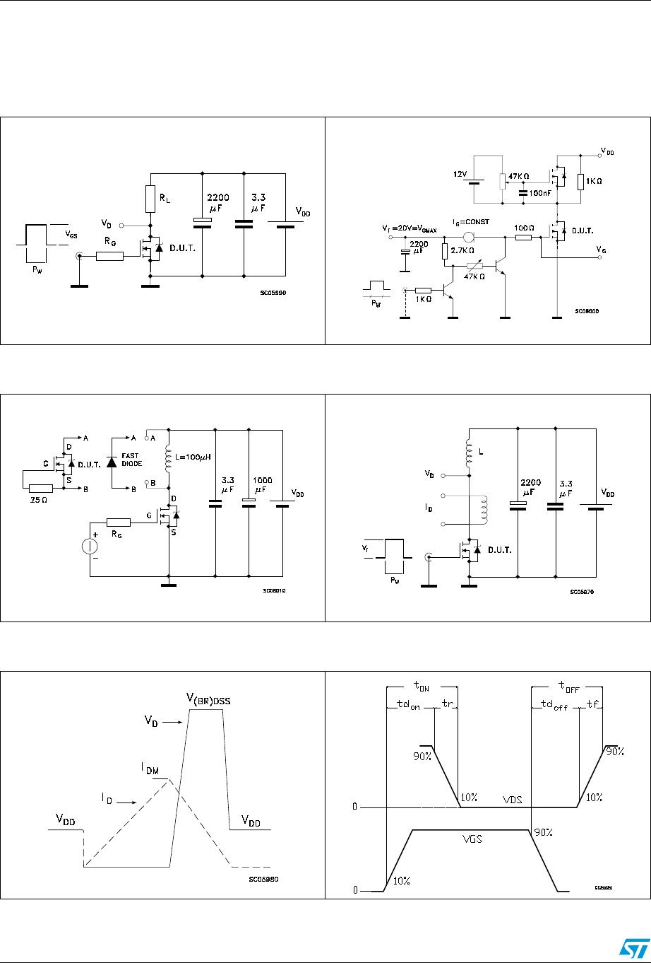
Figure 12.
Switching times
test ci
rcuit for
resistive load
Figure
13.
Gate charge test circuit
Figure 14.
T
e
st circuit
for inductive l
oad
switch
ing and diode recovery
times
Figure
15.
Unclam
ped
inductive
load tes
t
circuit
Figure 1
6.
Unclamped
inducti
ve wavefo
rm
Figure
17.
Switch
ing time
wavefor
m
STP80
NF10F
P
Packag
e mechani
cal data
9/12
4 Package
mecha
nical
dat
a
In order t
o meet environmen
tal r
equirem
ents,
ST offers these
d
evices in ECOP
ACK®
packages. Thes
e packages
have
a L
ead-free s
econd
level i
nterconnect
. The c
ategory
of
second level interconnect is marked on the package and on the i
nner box label, in
compliance
with JEDE
C S
t
andard J
ESD97.
The
maximum
ratings
related to s
oldering
conditions are also marked on the inner box label. ECOP
ACK is an ST trademark.
ECOP
A
CK sp
ecifications are available at:
www
.st.
com
P1-P3
P4-P6
P7-P9
P10-P12
STP80NF10FP
Mfr. #:
Buy STP80NF10FP
Manufacturer:
STMicroelectronics
Description:
MOSFET N Ch 100V 0.012 Ohm 30A
Lifecycle:
New from this manufacturer.
Delivery:
DHL
FedEx
Ups
TNT
EMS
Payment:
T/T
Paypal
Visa
MoneyGram
Western
Union
Products related to this Datasheet
STP80NF10FP