74HC161 All information provided in this document is subject to legal disclaimers. © NXP Semiconductors N.V. 2017. All rights reserved.
Product data sheet Rev. 3 — 4 January 2017 3 of 20
NXP Semiconductors
74HC161
Presettable synchronous 4-bit binary counter; asynchronous reset
Fig 4. Logic diagram
74HC161 All information provided in this document is subject to legal disclaimers. © NXP Semiconductors N.V. 2017. All rights reserved.
Product data sheet Rev. 3 — 4 January 2017 4 of 20
NXP Semiconductors
74HC161
Presettable synchronous 4-bit binary counter; asynchronous reset
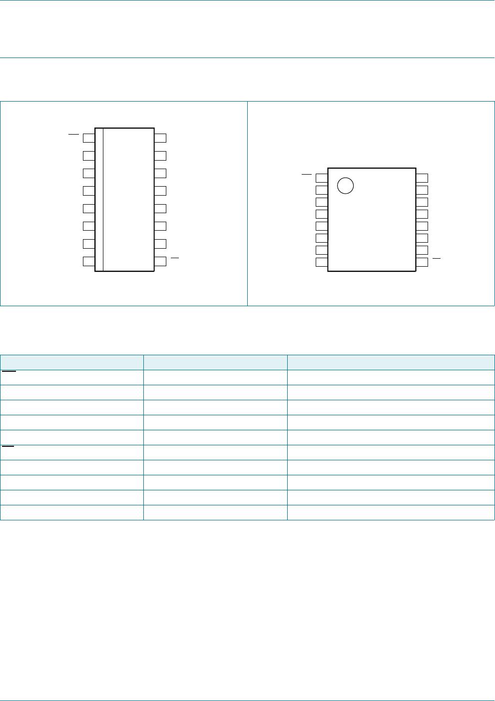
5. Pinning information
5.1 Pinning
5.2 Pin description
Fig 5. Pin configuration SO16 Fig 6. Pin configuration TSSOP16 and SSOP16
+&
0
5
9
&&
&
3
7&
'
4
'
4
'
4
'
4
&(3 &(7
*1' 3(
DDD







+&
0
5
9
&&
&
3
7&
'
4
'
4
'
4
'
4
&(3 &(7
*1' 3(
DDD







Table 2. Pin description
Symbol Pin Description
MR
1 asynchronous master reset (active LOW)
CP 2 clock input (LOW-to-HIGH, edge-triggered)
D0, D1, D2, D3 3, 4, 5, 6 data input
CEP 7 count enable input
GND 8 ground (0 V)
PE
9 parallel enable input (active LOW)
CET 10 count enable carry input
Q0, Q1, Q2, Q3 14, 13, 12, 11 flip-flop output
TC 15 terminal count output
V
CC
16 supply voltage
74HC161 All information provided in this document is subject to legal disclaimers. © NXP Semiconductors N.V. 2017. All rights reserved.
Product data sheet Rev. 3 — 4 January 2017 5 of 20
NXP Semiconductors
74HC161
Presettable synchronous 4-bit binary counter; asynchronous reset
6. Functional description
[1] H = HIGH voltage level
h = HIGH voltage level one set-up time prior to the LOW-to-HIGH clock transition
L = LOW voltage level
l = LOW voltage level one set-up time prior to the LOW-to-HIGH clock transition
q
n
= lower case letters indicate the state of the referenced output one set-up time prior to the LOW-to-HIGH clock transition
X = don’t care
= LOW-to-HIGH clock transition
[2] The TC output is HIGH when CET is HIGH and the counter is at terminal count (HHHH)
Table 3. Function table
[1]
Operating
modes
Input Output
MR CP CEP CET PE Dn Qn TC
Reset (clear)LXXXXXLL
Parallel load H XXl l LL
H XXl hH
[2]
Count H hhhXcount
[2]
Hold
(do nothing)
HX l X h X q
n
[2]
HX X l h X q
n
L
Fig 7. State diagram
DDD




 

74HC161D,653

Mfr. #:
Manufacturer:
Nexperia
Description:
Counter ICs SYNC 4-BIT BINARY COUNTER
Lifecycle:
New from this manufacturer.
Delivery:
DHL FedEx Ups TNT EMS
Payment:
T/T Paypal Visa MoneyGram Western Union