DocID13862 Rev 3 7/18
L6384E Electrical characteristics
18
4 Electrical characteristics
4.1 AC operation
4.2 DC operation
Table 5. AC operation electrical characteristics (V
CC
= 14.4 V; T
J
= 25 °C)
Symbol Pin Parameter Test condition Min. Typ. Max. Unit
t
on
1 vs. 5, 7
High/low-side driver turn-on
propagation delay
V
OUT
= 0 V R
dt
= 47 k
200+
dt
ns
t
onsd
3 vs. 5, 7
Shutdown input propagation
delay
220 280 ns
t
off
1 vs. 5, 7
High/low-side driver turn-off
propagation delay
V
OUT
= 0 V R
dt
= 47 k 250 300 ns
V
OUT
= 0 V R
dt
= 146 k 200 250 ns
V
OUT
= 0 V R
dt
= 270 k 170 200 ns
t
r
5, 7 Rise time C
L
= 1000 pF 50 ns
t
f
5, 7 Fall time C
L
= 1000 pF 30 ns
Table 6. DC operation electrical characteristics (V
CC
= 14.4 V; T
J
= 25 °C)
Symbol Pin Parameter Test condition Min. Typ. Max. Unit
Supply voltage section
V
clamp
2 Supply voltage clamping I
s
= 5 mA 14.6 15.6 16.6 V
V
CCth1
2 V
CC
UV turn-on threshold 11.5 12 12.5 V
V
CCth2
2
V
CC
UV turn-off threshold 9.5 10 10.5 V
V
CChys
V
CC
UV hysteresis 2 V
I
QCCU
Undervoltage quiescent supply
current
V
CC
11 V 150 A
I
QCC
Quiescent current V
IN
= 0 380 500 A
Bootstrapped supply voltage section
V
BOOT
8
Bootstrap supply voltage 17 V
I
QBS
Quiescent current IN = HIGH 100 A
I
LK
High voltage leakage current V
hvg
= V
OUT
= V
BOOT
= 600 V 10 A
R
dson
Bootstrap driver on-resistance
(1)
V
CC
12.5 V; IN = LOW 125
High/low-side driver
I
so
5, 7
Source short-circuit current V
IN
= V
ih
(t
p
< 10 s) 300 400 mA
I
si
Sink short-circuit current V
IN
= V
il
(t
p
< 10 s) 500 650 mA
Electrical characteristics L6384E
8/18 DocID13862 Rev 3
4.3 Timing diagram
Figure 3. Input/output timing diagram
Symbol Pin Parameter Test condition Min. Typ. Max. Unit
Logic inputs
V
il
1, 3
Low level logic threshold voltage 1.5 V
V
ih
High level logic threshold
voltage
3.6 V
I
ih
High level logic input current V
IN
= 15 V 50 70 A
I
il
Low level logic input current V
IN
= 0 V 1 A
I
ref
3 Deadtime setting current 28 A
dt 3 vs. 5, 7 Deadtime setting range
(2)
R
dt
= 47 k
R
dt
= 146 k
R
dt
= 270 k
0.4 0.5
1.5
2.7 3.1
s
s
s
V
dt
3 Shutdown threshold 0.5 V
1. R
DS(on)
is tested in the following way:
Where I
1
is the pin 8 current when V
BOOT
= V
BOOT1
, I
2
when V
BOOT
= V
BOOT2
.
2. The pin 3 is a high impedance pin. Therefore dt can be set also forcing a certain voltage V
3
on this pin. The deadtime is the
same obtained with an R
dt
if it is: R
dt
× I
ref
= V
3
.
Table 6. DC operation electrical characteristics (continued) (V
CC
= 14.4 V; T
J
= 25 °C)
R
DSON
V
CC
V
BOOT1
V
CC
V
BOOT2

I
1
V
CC
,V
BOOT1
I
2
V
CC
,V
BOOT2

-----------------------------------------------------------------------------------------------=
IN
SD
HVG
LVG
D99IN1017
DocID13862 Rev 3 9/18
L6384E Bootstrap driver
18
5 Bootstrap driver
A bootstrap circuitry is needed to supply the high voltage section. This function is normally
accomplished by a high voltage fast recovery diode (Figure 4 a). In the L6384E device
a patented integrated structure replaces the external diode. It is realized by a high voltage
DMOS, driven synchronously with the low-side driver (LVG), with a diode in series, as
shown in Figure 4 b. An internal charge pump (Figure 4 b) provides the DMOS driving
voltage. The diode connected in series to the DMOS has been added to avoid undesirable
turn-on.
C
BOOT
selection and charging
To choose the proper C
BOOT
value the external MOSFET can be seen as an equivalent
capacitor. This capacitor C
EXT
is related to the MOSFET total gate charge:
Equation 1
The ratio between the capacitors C
EXT
and C
BOOT
is proportional to the cyclical voltage loss.
It has to be:
C
BOOT
>>>C
EXT
E.g.: if Q
gate
is 30 nC and V
gate
is 10 V, C
EXT
is 3 nF. With C
BOOT
= 100 nF the drop would be
300 mV.
If HVG has to be supplied for a long time, the C
BOOT
selection has to take into account also
the leakage losses.
E.g.: HVG steady state consumption is lower than 100 A, so if HVG T
ON
is 5 ms, C
BOOT
has to supply 0.5 C to C
EXT
. This charge on a 1 F capacitor means a voltage drop of
0.5 V.
The internal bootstrap driver gives great advantages: the external fast recovery diode can
be avoided (it usually has a great leakage current).
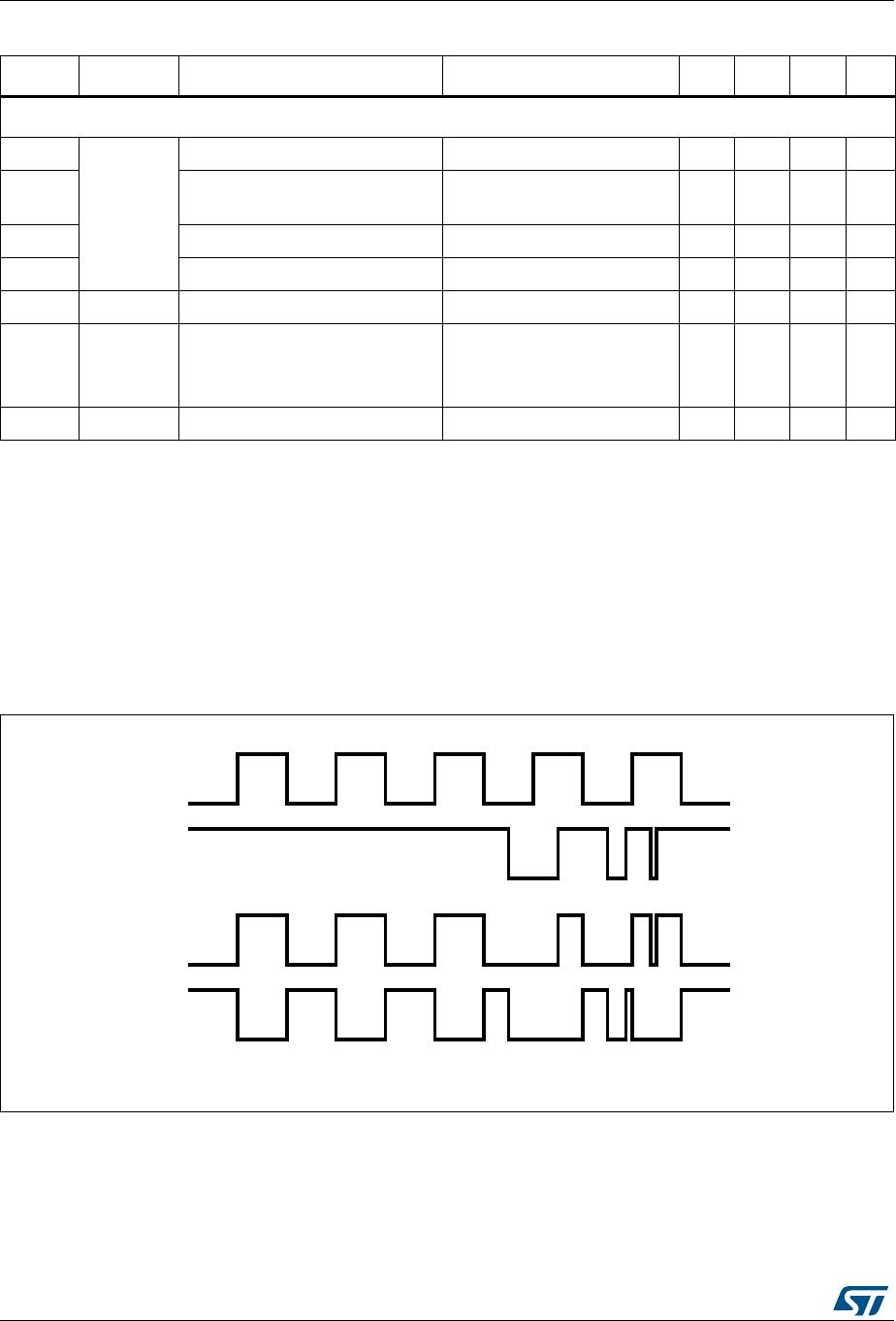
This structure can work only if V
OUT
is close to GND (or lower) and in the meanwhile the
LVG is on. The charging time (T
charge
) of the C
BOOT
is the time in which both conditions are
fulfilled and it has to be long enough to charge the capacitor.
The bootstrap driver introduces a voltage drop due to the DMOS R
DSON
(typical value:
125 ). At low frequency this drop can be neglected. Anyway increasing the frequency it
must be taken in to account.
The following equation is useful to compute the drop on the bootstrap DMOS:
Equation 2
where Q
gate
is the gate charge of the external power MOSFET, R
dson
is the on-resistance of
the bootstrap DMOS, and T
charge
is the charging time of the bootstrap capacitor.
C
EXT
Q
gate
V
gate
-------------- -=
V
drop
I
ch earg
R
dson
V
drop
Q
gate
T
ch earg
------------------- R
dson
==

L6384E

Mfr. #:
Manufacturer:
STMicroelectronics
Description:
Gate Drivers HV H-Bridge drive
Lifecycle:
New from this manufacturer.
Delivery:
DHL FedEx Ups TNT EMS
Payment:
T/T Paypal Visa MoneyGram Western Union

Products related to this Datasheet