BATTERY PROTECTION IC FOR 3-SERIAL- OR 4-SERIAL-CELL PACK
S-8254A Series
Rev.5.0_01
Seiko Instruments Inc.
4
2. Product Name List
Table 1
Product name /
Item
Overcharge
detection voltage
[V
CU
]
Overcharge
release voltage
[V
CL
]
Overdischarge
detection voltage
[V
DL
]
Overdischarge
release voltage
[V
DU
]
Overcurrent
detection voltage 1
[V
IOV1
]
0 V battery
charge function
S-8254AAAFT-TB-x
4.350
±
0.025 V 4.150
±
0.050 V 2.00
±
0.080 V 2.70
±
0.100 V 0.30
±
0.025 V
Available
S-8254AABFT-TB-x
4.250
±
0.025 V 4.250
±
0.025 V 2.00
±
0.080 V 2.70
±
0.100 V 0.30
±
0.025 V
Available
S-8254AAEFT-TB-x
4.350
±
0.025 V 4.150
±
0.050 V 2.00
±
0.080 V 2.70
±
0.100 V 0.20
±
0.025 V
Available
S-8254AAFFT-TB-x
4.350
±
0.025 V 4.150
±
0.050 V 2.40
±
0.080 V 3.00
±
0.100 V 0.20
±
0.025 V
Available
S-8254AAGFT-TB-x
4.275
±
0.025 V 4.075
±
0.050 V 2.30
±
0.080 V 2.70
±
0.100 V 0.13
±
0.025 V
Available
S-8254AAHFT-TB-x
4.350
±
0.025 V 4.150
±
0.050 V 2.40
±
0.080 V 2.70
±
0.100 V 0.10
±
0.025 V
Available
S-8254AAIFT-TB-x
4.350
±
0.025 V 4.150
±
0.050 V 2.40
±
0.080 V 3.00
±
0.100 V 0.30
±
0.025 V
Available
S-8254AAJFT-TB-x
4.350
±
0.025 V 4.150
±
0.050 V 2.40
±
0.080 V 3.00
±
0.100 V 0.15
±
0.025 V
Available
S-8254AAKFT-TB-x
4.350
±
0.025 V 4.150
±
0.050 V 2.70
±
0.080 V 3.00
±
0.100 V 0.20
±
0.025 V
Available
S-8254AALFT-TB-x
4.300
±
0.025 V 4.150
±
0.050 V 2.40
±
0.080 V 3.00
±
0.100 V 0.20
±
0.025 V
Available
S-8254AAMFT-TB-x
4.200
±
0.025 V 4.100
±
0.050 V 2.50
±
0.080 V 2.70
±
0.100 V 0.30
±
0.025 V
Available
S-8254AANFT-TB-x
4.250
±
0.025 V 4.150
±
0.050 V 2.50
±
0.080 V 3.00
±
0.100 V 0.10
±
0.025 V
Available
S-8254AAOFT-TB-X
4.300
±
0.025 V 4.080
±
0.050 V 2.50
±
0.080 V 3.00
±
0.100 V 0.10
±
0.025 V
Available
S-8254AAPFT-TB-x
4.280
±
0.025 V 4.130
±
0.050 V 3.00
±
0.080 V 3.00
±
0.080 V 0.15
±
0.025 V
Available
S-8254AAQFT-TB-x
3.900
±
0.025 V 3.800
±
0.050 V 2.30
±
0.080 V 2.70
±
0.100 V 0.30
±
0.025 V
Available
S-8254AARFT-TB-x
4.350
±
0.025 V 4.150
±
0.050 V 2.80
±
0.080 V 3.00
±
0.100 V 0.20
±
0.025 V
Available
S-8254AASFT-TB-x
4.290
±
0.025 V
4.090
±
0.050 V 2.30
±
0.080 V 3.00
±
0.100 V 0.075
±
0.025 V
Available
S-8254AATFT-TB-x
4.200
±
0.025 V
4.200
±
0.025 V 2.00
±
0.080 V 2.70
±
0.100 V 0.30
±
0.025 V
Available
S-8254AAUFT-TB-x
4.350
±
0.025 V
4.150
±
0.050 V 2.40
±
0.080 V 3.00
±
0.100 V 0.20
±
0.025 V
Unavailable
S-8254AAVFT-TB-x
4.250
±
0.025 V 4.150
±
0.050 V 2.70
±
0.080 V 3.00
±
0.100 V 0.20
±
0.025 V
Available
S-8254AAWFT-TB-x
4.250
±
0.025 V 4.100
±
0.050 V 3.00
±
0.080 V 3.20
±
0.100 V 0.10
±
0.025 V
Unavailable
S-8254AAXFT-TB-x
4.250
±
0.025 V 4.100
±
0.050 V 2.00
±
0.080 V 2.70
±
0.100 V 0.15
±
0.025 V
Available
S-8254AAYFT-TB-x
4.275
±
0.025 V 4.125
±
0.050 V 2.40
±
0.080 V 2.70
±
0.100 V 0.10
±
0.025 V
Available
S-8254AAZFT-TB-x
4.250
±
0.025 V 4.150
±
0.050 V 2.00
±
0.080 V 2.70
±
0.100 V 0.13
±
0.025 V
Available
S-8254ABAFT-TB-x
3.900
±
0.025 V 3.800
±
0.050 V 2.00
±
0.080 V 2.50
±
0.100 V 0.15
±
0.025 V
Available
S-8254ABBFT-TB-x
4.200
±
0.025 V 4.200
±
0.025 V 2.50
±
0.080 V 3.20
±
0.100 V 0.30
±
0.025 V
Available
S-8254ABCFT-TB-x
4.175
±
0.025 V 3.975
±
0.050 V 2.75
±
0.080 V 3.05
±
0.100 V 0.10
±
0.025 V
Available
S-8254ABDFT-TB-y
4.300
±
0.025 V 4.100
±
0.050 V 2.00
±
0.080 V 2.00
±
0.080 V 0.13
±
0.025 V
Available
S-8254ABEFT-TB-y
4.200
±
0.025 V 4.150
±
0.050 V 2.50
±
0.080 V 3.00
±
0.100 V 0.15
±
0.025 V
Available
S-8254ABFFT-TB-x
4.150
±
0.025 V 4.050
±
0.050 V 2.00
±
0.080 V 2.70
±
0.100 V 0.13
±
0.025 V
Available
S-8254ABGFT-TB-x
4.180
±
0.025 V 4.080
±
0.050 V 2.00
±
0.080 V 2.70
±
0.100 V 0.13
±
0.025 V
Available
S-8254ABHFT-TB-y
4.150
±
0.025 V 4.050
±
0.050 V 2.50
±
0.080 V 2.80
±
0.100 V 0.10
±
0.025 V
Available
S-8254ABIFT-TB-x
4.215
±
0.025 V 4.115
±
0.050 V 2.40
±
0.080 V 3.00
±
0.100 V 0.20
±
0.025 V
Unavailable
Remark 1. Please contact our sales office for the products with the detection voltage value other than those
specified above.
2. x: G or U
y: S or U
3. Please select products of environmental code = U for Sn 100%, halogen-free products.
BATTERY PROTECTION IC FOR 3-SERIAL- OR 4-SERIAL-CELL PACK
Rev.5.0_01
S-8254A Series
Seiko Instruments Inc.
5
Pin Configuration
16-Pin TSSOP
Top view
8
7
6
5
3
2
4
1
11
16
9
10
12
14
15
13
COP
VMP
DOP
VINI
CDT
CCT
VSS
NC
VDD
VC1
VC2
VC3
VC4
CTL
SEL
NC
Figure 2
Table 2
Pin No. Symbol Description
1 COP FET gate connection pin for charge control (Nch open drain output)
2 VMP
Pin for voltage detection between VC1 and VMP (Pin for overcurrent 3
detection)
3 DOP FET gate connection pin for discharge control FET (CMOS output)
4 VINI
Pin for voltage detection between VSS and VINI (Pin for overcurrent detection
1,2)
5 CDT
Capacitor connection pin for delay for overdischarge detection, delay for
overcurrent detection 1
6 CCT Capacitor connection pin for delay for overcharge current
7 VSS
Input pin for negative power supply,
Connection pin for battery 4’s negative voltage
8 NC
*1
No connection
9 NC
*1
No connection
10 SEL
Pin for switching 3-series or 4-series cell
V
SS
level: 3-series cell, V
DD
level : 4-series cell
11 CTL Control of charge FET and discharge FET
12 VC4
Connection pin for battery 3’s negative voltage,
Connection pin for battery 4’s positive voltage
13 VC3
Connection pin for battery 2’s negative voltage,
Connection pin for battery 3’s positive voltage
14 VC2
Connection pin for battery 1’s negative voltage,
Connection pin for battery 2’s positive voltage
15 VC1 Connection pin for battery 1’s positive voltage
16 VDD
Input pin for positive power supply,
Connection pin for battery 1’s positive voltage
*1. The NC pin is electrically open. The NC pin can be connected to VDD or VSS.
BATTERY PROTECTION IC FOR 3-SERIAL- OR 4-SERIAL-CELL PACK
S-8254A Series
Rev.5.0_01
Seiko Instruments Inc.
6
Absolute Maximum Ratings
Table 3
(Ta = 25°C unless otherwise specified
)
Item Symbol Applied pin Absolute Maximum Ratings Unit
Input voltage between VDD and VSS V
DS
V
SS
0.3 to V
SS
+ 26
V
Input pin voltage V
IN
VC1, VC2, VC3,
VC4, CTL, SEL,
CCT, CDT, VINI
V
SS
0.3 to V
DD
+ 0.3
V
VMP pin input voltage V
VMP
VMP
V
SS
0.3 to V
SS
+ 26
V
DOP pin output voltage V
DOP
DOP
V
SS
0.3 to V
DD
+ 0.3
V
COP pin output voltage V
COP
COP
V
SS
0.3 to V
SS
+ 26
V
400 (When not mounted on board) mW
Power dissipation P
D
1100
*1
mW
Operating ambient temperature T
opr
40 to + 85 °C
Storage temperature T
stg
40 to + 125 °C
*1. When mounted on board
[Mounted board]
(1) Board size : 114.3 mm × 76.2 mm × t1.6 mm
(2) Board name : JEDEC STANDARD51-7
Caution The absolute maximum ratings are rated values exceeding which the product could suffer
physical damage. These values must therefore not be exceeded under any conditions.
0
50 100
150
800
400
0
Power Dissipation (P
D
) [mW]
Ambient Temperature (Ta) [°C]
1000
600
200
1200
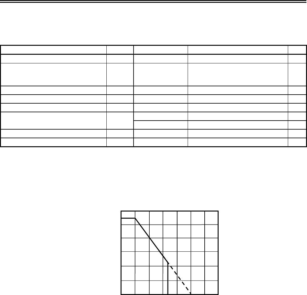
Figure 3 Power Dissipation of Package (When Mounted on Board)

S-8254AALFT-TB-G

Mfr. #:
Manufacturer:
Description:
Battery Management Lithium-Ion battery protection 3/4 cell
Lifecycle:
New from this manufacturer.
Delivery:
DHL FedEx Ups TNT EMS
Payment:
T/T Paypal Visa MoneyGram Western Union