LT3081
10
3081fc
For more information www.linear.com/LT3081
block DiagraM
+
50µA
IN
I
MON
TEMPERATURE
DEPENDENT
CURRENT SOURCE
1µA/°C
SET I
LIM
OUT
3081 BD
PROGRAMMABLE
CURRENT LIMIT
CURRENT
MONITOR
I
MON
= I
LOAD
/5000
TEMP
pin FuncTions
IN: Input. This pin supplies power to regulate internal
circuitry and supply output load current. For the device
to operate properly and regulate, the voltage on this pin
must be between the dropout voltage and 36V above the
OUT pin (depending on output load current, see Dropout
Voltage Specifications).
OUT: Output. This is the power output of the device. The
LT3081 requires a 5mA minimum load current for proper
output regulation.
TEMP: Temperature Output. This pin delivers a current
proportional to the internal average junction temperature.
Current output isA/°C for temperatures aboveC. The
TEMP pin output current typically equals 25µA at 25°C.
The output of the TEMP pin is valid for voltages from V
OUT
+ 0.4V to V
OUT
– 40V. If unused, connect this pin to OUT.
I
LIM
: Current Limit Program. A resistor between this pin
and OUT programs output current limit to a level propor-
tional to
resistor value. Connect this resistor directly to
OUT
at the pins of the package. The typical ratio of current
limit to resistor value is 360mA/kΩ with a 450Ω offset.
If programmable current limit is not used, leave this pin
open; the internal current limit of
the LT3081 is still active,
keeping
the device inside safe operating limits. External
voltage drops between the current limit resistor and V
OUT
will affect the current limit. Keep drops below 1mV.
I
MON
: Output Current Monitor. The I
MON
pin sources a
current typically equal to I
LOAD
/5000 or 200µA per amp of
output current. Terminating this pin with a resistor to GND
produces a voltage proportional to I
LOAD
. For example,
at I
LOAD
= 1.5A, I
MON
typically sources 300µA. With a
1k resistor to GND, this produces 300mV. The output
of the I
MON
pin is valid for voltages from V
OUT
+ 0.4V to
V
OUT
– 40V. If unused, connect this pin to OUT.
SET: Set. This pin is the error amplifier’s noninverting
input and also sets the operating bias point of the circuit.
A fixed 50μA current source flows out of this pin. A single
external resistor programs V
OUT
. Output voltage range is
0V to 34.5V.
Exposed Pad/Tab: Output. The exposed pad of the DF and
FE packages and the tab of the R and T7 packages are tied
internally to OUT. As such, tie them directly to OUT (Pins
1-4/Pins 1-5, 8, 9, 16/Pin 4/Pin 4) at the
PCB. The amount
of
copper area and planes connected to OUT determine
the effective thermal resistance of the packages.
NC: No Connection. No connect pins have no connection
to internal circuitry and may be tied to IN, OUT, GND or
floated.
LT3081
11
3081fc
For more information www.linear.com/LT3081
applicaTions inForMaTion
Introduction
The LT3081 regulator is easy to use and has all the pro-
tection features
expected in high performance regulators.
Included are short-circuit protection, reverse-input protec-
tion and
safe operating area protection, as well as thermal
shutdown
with hysteresis. Safe operating area (SOA) for
the LT3081 is extended, allowing for use in harsh indus
-
trial and automotive environments where sudden spikes
in input voltage lead to high power dissipation.
The LT3081 fits well in applications needing multiple rails.
This new architecture adjusts down to zero with a single
resistor, handling modern low voltage digital ICs as well
as allowing easy parallel operation and thermal manage
-
ment without heat sinks. Adjusting to zero output allows
shutting off the powered circuitry.
A precision “0” TC 50μA reference current source connects
to the noninverting input of a power operational amplifier.
The power operational amplifier provides a low impedance
buffered output to the voltage on the noninverting input.
A single resistor from the noninverting input to ground
sets the output voltage. If this resistor is set to 0Ω, zero
output voltage results. Therefore, any output voltage can
be obtained between zero and the maximum defined by
the input power supply is
obtainable.
The
benefit of using a true internal current source as the
reference, as opposed to a bootstrapped reference in older
regulators, is not so obvious in this architecture. A true
reference current source allows the regulator to have gain
and frequency response independent of the impedance on
the positive input. On older adjustable regulators, such as
the LT1086 loop gain changes with output voltage and
bandwidth changes if the adjustment pin is bypassed to
ground. For the LT3081, the loop gain is unchanged with
output voltage changes or bypassing. Output regulation
is not a fixed percentage of output voltage, but is a fixed
fraction of millivolts. Use of a true current source allows
all of the gain in the buffer amplifier to provide regulation,
and none of that gain is needed to amplify up the reference
to a higher output voltage.
The LT3081 has many additional features that facilitate
monitoring and control. Current limit is externally pro
-
grammable via a single resistor between the I
LIM
pin and
OUT. Shorting this resistor out disables all output current
to the load, only bias currents remain.
The I
MON
pin produces a current output proportional to
load current. For every 1A of load current, the I
MON
pin
sources 200µA of current. This can be sensed using an
external resistor to monitor load requirements and detect
potential faults. The I
MON
pin can operate at voltages above
OUT, so it operates even during a short-circuit condition.
One additional monitoring function is the TEMP pin, a cur
-
rent source that is proportional to average die temperature.
For die temperatures aboveC, the TEMP pin sources a
current equal toA/°C. This pin operates normally during
output short-circuit conditions.
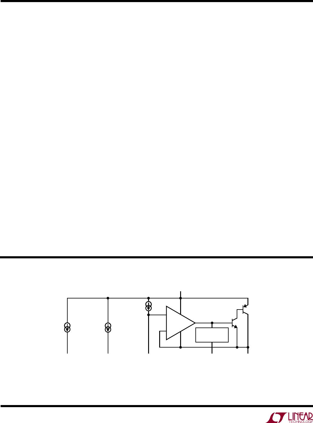
Programming Linear Regulator Output Voltage
The LT3081 generates a 50μA reference current that flows
out of the SET pin. Connecting a resistor from SET to
ground generates a voltage that becomes the reference
point for the error amplifier (see Figure 1). The reference
voltage equals 50µA multiplied by the value of the SET
pin resistor. Any voltage can be generated and there is
no minimum output voltage for the regulator.
3081 F01
IN
SET OUT
+
LT3081
50µA
R
LOAD
C
SET
R
SET
C
IN
V
OUT
= 50µA • R
SET
C
OUT
Figure 1. Basic Adjustable Regulator
LT3081
12
3081fc
For more information www.linear.com/LT3081
applicaTions inForMaTion
Table 1 lists many common output voltages and the clos-
est standard 1%
resistor values used to generate that
output voltage.
Regulation of the output voltage requires a minimum load
current of 5mA. For true zero voltage output operation,
return this 5mA load current to a negative output voltage.
Table 1. 1% Resistors for Common Output Voltages
V
OUT
(V) R
SET
(kΩ)
1 20
1.2 24.3
1.5 30.1
1.8 35.7
2.5 49.9
3.3 66.5
5 100
With the 50µA current source used to generate the reference
voltage, leakage paths to or from the SET pin can create
errors in the reference and output voltages. High quality
insulation should be used (e.g., Teflon, Kel-F); cleaning of
all insulating surfaces to remove fluxes and other residues
is required. Surface coating may be necessary to provide
a moisture barrier in high humidity environments.
Minimize board leakage by encircling the SET pin and
circuitry with a guard ring operated at a potential close
to itself. Tie the guard ring to the OUT pin. Guarding both
sides of the circuit board is required. Bulk leakage reduction
depends on
the guard ring width. 50nA of leakage into or
out
of the SET pin and its associated circuitry creates a
0.1% reference voltage error. Leakages of this magnitude,
coupled with other sources of leakage, can cause signifi
-
cant offset voltage and reference drift, especially over the
possible
operating temperature range. Figure 2 depicts an
example guard ring layout.
If guard ring techniques are used, this bootstraps any
stray capacitance at the SET pin. Since the
SET pin is
a
high impedance node, unwanted signals may couple
into the SET pin and cause erratic behavior. This will
be most noticeable when operating with minimum
output capacitors at full load current. The easiest way
to remedy this is to bypass the SET pin with a small
amount of capacitance from SET to ground, 10pF to
20pF is sufficient.
Configuring the LT3081 as a Current Source
Setting the LT3081 to operate as a 2-terminal current
source is a simple matter. The 50µA reference current from
the SET pin is used with one resistor to generate a small
voltage, usually in the range of 100mV to 1V (200mV is a
level that rejects offset voltage, line regulation, and other
errors without being excessively large). This voltage is
then applied across a second resistor that connect from
OUT to the first resistor. Figure 3 shows connections and
formulas to calculate a basic current source configuration.
3081 F02
SET PIN
GND
OUT
Figure 2. Guard Ring Layout Example of DF Package Figure 3. Using the LT3081 as a Current Source
I
OUT
5mA
V
SET
= 50µA R
SET
I
OUT
=
V
SET
R
OUT
=
50µA R
SET
R
OUT
IN
SET OUT
+
LT3081
50µA
I
OUT
V
SET
R
SET
3081 F03
+
R
OUT

LT3081IR#PBF

Mfr. #:
Manufacturer:
Analog Devices / Linear Technology
Description:
LDO Voltage Regulators 1.5A Single Resistor Programmable Rugged Linear Regulator
Lifecycle:
New from this manufacturer.
Delivery:
DHL FedEx Ups TNT EMS
Payment:
T/T Paypal Visa MoneyGram Western Union