LT3081
19
3081fc
For more information www.linear.com/LT3081
Connecting a resistor from I
MON
to ground converts the
I
MON
pin current into a voltage to allow for monitoring by
an ADC. With a 1k resistor, 0mV to 300mV indicates 0A
to 1.5A of load current.
Compensating for Cable Drops with I
MON
The I
MON
pin can compensate for resistive drops in wires
or cables between the LT3081 and the load. Breaking the
SET resistor into two pieces adjusts the output voltage as a
function of load current. The ratio of the output wire/cable
impedance to the bottom resistor should be 1:5000. The
sum total of the two SET resistor values determines the
initial output voltage. Figure 11 shows a typical application
and formulas for calculating resistor values.
PC board, copper traces and planes. Surface mount heat
sinks, plated through-holes and solder-filled vias can also
spread the heat generated by power devices.
Junction-to-case thermal resistance is specified from the
IC junction to the bottom of the case directly, or the bot
-
tom of the pin most directly in the heat path. This is the
lowest thermal resistance path for heat flow. Only proper
device mounting ensures the best possible thermal flow
from this area of
the packages to the heat sinking material.
Note that the exposed pad of the DFN and TSSOP pack-
ages and
the tab of the DD-Pak and TO-220 packages
are electrically connected to the output (V
OUT
).
Tables 3 through 5 list thermal resistance as a function
of copper areas on a fixed board size. All measurements
were taken in still air on a 4-layer FR-4 board with 1oz
solid internal planes and 2oz external trace planes with a
total finished board thickness of 1.6mm.
Table 3. DF Package, 12-Lead DFN
COPPER AREA
BOARD AREA
THERMAL RESISTANCE
(JUNCTION-TO-AMBIENT)TOPSIDE* BACKSIDE
2500mm
2
2500mm
2
2500mm
2
18°C/W
1000mm
2
2500mm
2
2500mm
2
22°C/W
225mm
2
2500mm
2
2500mm
2
29°C/W
100mm
2
2500mm
2
2500mm
2
35°C/W
*Device is mounted on topside
Table 4. FE Package, 16-Lead TSSOP
COPPER AREA
BOARD AREA
THERMAL RESISTANCE
(JUNCTION-TO-AMBIENT)TOPSIDE* BACKSIDE
2500mm
2
2500mm
2
2500mm
2
16°C/W
1000mm
2
2500mm
2
2500mm
2
20°C/W
225mm
2
2500mm
2
2500mm
2
26°C/W
100mm
2
2500mm
2
2500mm
2
32°C/W
*Device is mounted on topside
Table 5. R Package, 7-Lead DD-Pak
COPPER AREA
BOARD AREA
THERMAL RESISTANCE
(JUNCTION-TO-AMBIENT)TOPSIDE* BACKSIDE
2500mm2 2500mm2 2500mm2 13°C/W
1000mm2 2500mm2 2500mm2 14°C/W
225mm2 2500mm2 2500mm2 16°C/W
*Device is mounted on topside
applicaTions inForMaTion
Figure 11. Using I
MON
to Compensate for Cable Drops
Thermal Considerations
The LT3081’s internal power and thermal limiting circuitry
protects itself under overload conditions. For continuous
normal load conditions, do not exceed the 125°C (E- and
I-grades) or 150°C (H- and MP-grades) maximum junc
-
tion temperature
.
Carefully consider all sources of thermal
resistance from junction-to-ambient. This includes (but is
not limited to) junction-to
-case, case-to-heat sink inter-
face,
heat sink resistance or circuit board-to-ambient as
the
application dictates. Consider all additional, adjacent
heat generating sources in proximity on the PCB.
Surface mount packages provide the necessary heat
sinking by using the heat spreading capabilities of the
LT3081
IN
C
IN
F
C
OUT
10µF
3081 F11
OUT
SET
R
SET
29.8k
R
COMP
= 5000 • R
CABLE(TOTAL)
V
OUT(LOAD)
= 50µA (R
SET
+ R
COMP
)
R
CABLE2
0.02Ω
R
CABLE
0.02Ω
R
COMP
200Ω
I
MON
LOAD
LT3081
20
3081fc
For more information www.linear.com/LT3081
applicaTions inForMaTion
T7 Package, 7-Lead TO-220
Thermal Resistance (Junction-to-Case) = 3°C/W
For further information on thermal resistance and using
thermal information, refer to JEDEC standard JESD51,
notably JESD51-12.
PCB layers, copper weight, board layout and thermal vias
affect the resultant thermal resistance. Tables 3 through 5
provide thermal resistance numbers for best-case 4-layer
boards with 1oz internal and 2oz external copper. Modern,
multilayer PCBs may not be able to achieve quite the same
level performance as found in these tables. Demo circuit
1870A’s board layout using multiple inner V
OUT
planes
and multiple thermal vias achieves 16°C/W performance
for the FE package.
Calculating Junction Temperature
Example: Given an output voltage of 0.9V, an IN voltage
of 2.5V ±5%, output current range from 10mA to 1A
and a maximum ambient temperature of 50°C, what is
the maximum junction temperature for the DD-Pak on a
2500mm2 board with topside copper of 1000mm
2
?
The power in the circuit equals:
P
TOTAL
= (V
IN
– V
OUT
)(I
OUT
)
The current delivered to the SET pin is negligible and can
be ignored.
V
IN(MAX_CONTINUOUS)
= 2.625V (2.5V + 5%)
V
OUT
= 0.9V, I
OUT
= 1A, T
A
= 50°C
Power dissipation under these conditions equals:
P
TOTAL
= (V
IN
– V
OUT
)(I
OUT
)
P
TOTAL
= (2.625V – 0.9V)(1A) = 1.73W
Junction Temperature equals:
T
J
= T
A
+ P
TOTAL
θ
JA
(using tables)
T
J
= 50°C + 1.73W • 14°C/W = 74.2°C
In this case, the junction temperature is below the maxi-
mum rating, ensuring reliable operation.
Reducing
Power Dissipation
In
some applications it may be necessary to reduce the
power dissipation in the LT3081 package without sacrificing
output current capability. Tw o techniques are available. The
first technique, illustrated in Figure 12, employs a resis
-
tor in
series with the regulator’s input. The voltage drop
across
R
S
decreases the LT3081’s IN-to-OUT differential
voltage and correspondingly decreases the LT3081’s
power dissipation.
As an example, assume: V
IN
= 7V, V
OUT
= 3.3V and I
OUT(MAX)
= 1.5A. Use the formulas from the Calculating Junction
Temperature section previously discussed.
Without series resistor R
S
, power dissipation in the
LT3081 equals:
P
TOTAL
= (7V – 3.3V) • 1.5A = 5.55W
If the voltage differential (V
DIFF
) across the LT3081 is
chosen as 1.5V, then R
S
equals:
R
S
=
7V 3.3V 1.5V
1.5A
= 1.5
Power dissipation in the LT3081 now equals:
P
TOTAL
= 1.5V • 1.5A = 2.25W
The LT3081’s power dissipation is now only 40% compared
to no series resistor. R
S
dissipates 3.3W of power. Choose
appropriate wattage resistors or use multiple resistors in
parallel to handle and dissipate the power properly.
3081 F12
IN
V
IN
SET OUT
+
LT3081
50µA
R
SET
R
S
V
OUT
V
IN
C2
C1
Figure 12. Reducing Power Dissipation Using a Series Resistor
LT3081
21
3081fc
For more information www.linear.com/LT3081
applicaTions inForMaTion
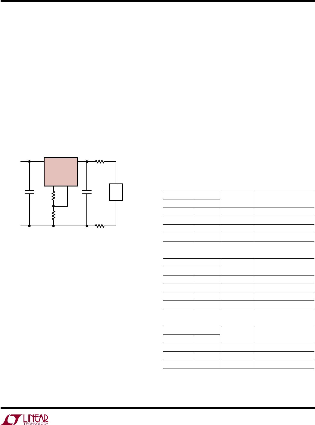
The second technique for reducing power dissipation,
shown in Figure 13, uses a resistor in parallel with the
LT3081. This resistor provides a parallel path for current
flow, reducing the current flowing through the LT3081.
This technique works well if input voltage is reasonably
constant and output load current changes are small. This
technique also increases the maximum available output
current at the expense of minimum load requirements.
R
P
dissipates 1.52W of power. As with the first technique,
choose appropriate wattage resistors to handle and dis-
sipate the
power properly. With this configuration, the
LT3081
supplies only 0.86A. Therefore, load current can
increase by 0.64A to a total output current of 2.14A while
keeping the LT3081 in its normal operating range.
High Temperature Operation
Care must be taken when designing the LT3081H/
LT3081MP applications to operate at high ambient tem
-
peratures. The LT3081
H/LT3081MP operates at high
temperatures, but erratic operation can occur due to un-
foreseen variations
in
external components. Some tantalum
capacitors are available for high temperature operation, but
ESR is often several ohms; capacitor ESR above 0.5Ω is
unsuitable for use with the LT3081H/LT3081MP. Multiple
ceramic capacitor manufacturers
now offer
ceramic capaci-
tors that are rated to 150°C using an X8R dielectric. Check
each
passive component for absolute value and voltage
ratings over the operating temperature range.
Leakages in capacitors or from solder flux left after insuf
-
ficient board cleaning adversely affects low current nodes,
such
as the SET, I
MON
, and TEMP pins. Consider junction
temperature increase due to power dissipation in both
the junction and nearby components to ensure maximum
specifications are not violated for the LT3081H/LT3081MP
or external components.
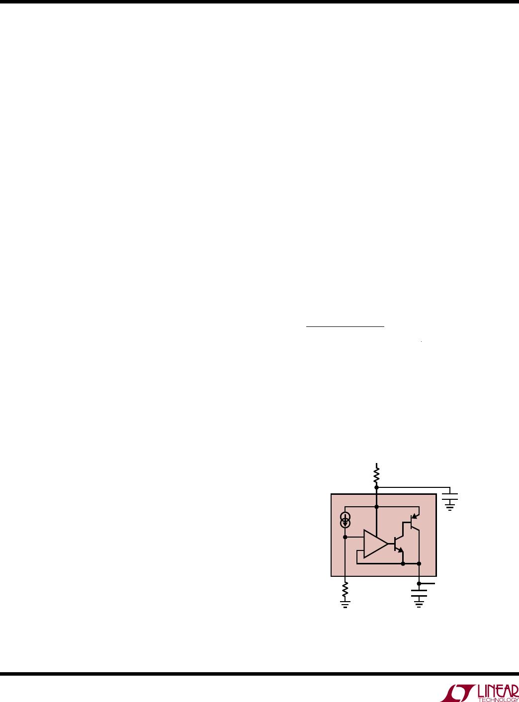
Protection Features
The LT3081 incorporates several protection features ideal
for harsh industrial and automotive environments, among
other applications. In addition to normal monolithic regula
-
tor protection features such as current limiting and thermal
limiting, the LT3081 protects itself against reverse-input
voltages, reverse-output voltages, and large OUT-to-SET
pin voltages.
Current limit protection and thermal overload protection
protect the IC against output current overload conditions.
For normal operation, do not exceed the rated absolute
maximum junction temperature. The thermal shutdown
circuit’s temperature threshold is typically 165°C and
incorporates about 5°C of hysteresis.
3081 F13
IN
SET OUT
+
LT3081
50µA
R
SET
V
OUT
V
IN
C2
C1
R
P
Figure 13. Reducing Power Dissipation Using a Parallel Resistor
As an example, assume: V
IN
= 5V, V
IN(MAX)
= 5.5V, V
OUT
= 3.3V, V
OUT(MIN)
= 3.2V, I
OUT(MAX)
= 1.5A and I
OUT(MIN)
= 0.7A. Also, assuming that R
P
carries no more than 90%
of I
OUT(MIN)
= 630mA.
Calculating R
P
yields:
R
P
=
5.5V 3.2V
0.63A
= 3.65
(5% Standard value = 3.6Ω)
The maximum total power dissipation is:
(5.5V – 3.2V) • 1.5A = 3.5W
However, the LT3081 supplies only:
1.5A
5.5V 3.2V
3.6
= 0.86A
Therefore, the LT3081’s power dissipation is only:
P
DISS
= (5.5V – 3.2V) • 0.86A = 1.98W

LT3081IR#PBF

Mfr. #:
Manufacturer:
Analog Devices / Linear Technology
Description:
LDO Voltage Regulators 1.5A Single Resistor Programmable Rugged Linear Regulator
Lifecycle:
New from this manufacturer.
Delivery:
DHL FedEx Ups TNT EMS
Payment:
T/T Paypal Visa MoneyGram Western Union