LT3081
16
3081fc
For more information www.linear.com/LT3081
applicaTions inForMaTion
In some extreme cases, capacitors or series RC networks
may be required on both the LT3081’s input and output to
stabilize the circuit. Figure 6 depicts a general application
using input and output capacitor networks rather than
an input-to-output capacitor. As the input of the current
source tends to be high impedance, placing a capacitor
on the input does not have the same effect as placing a
capacitor on the lower impedance output. Capacitors in the
range of 0.1µF toF usually provide sufficient bypassing
on the input, and the value of input capacitance may be
increased without limit. Pay careful attention to using low
ESR input capacitors with long input lines (see the Stabil
-
ity and Input Capacitance section for more information).
Using Ceramic Capacitors
Give extra consideration to the use of ceramic capacitors.
Ceramic capacitors are manufactured with a variety of di
-
electrics, each with different behavior across temperature
and applied voltage. The most common dielectrics used
are specified with EIA temperature characteristic codes of
Z5U, Y5V, X5R and X7R. The Z5U and Y5V dielectrics are
good for providing high capacitances in a small package,
but they tend
to have strong voltage and temperature
coefficients
as shown in Figures 7 and 8. When used with
a 5V regulator, a 16V 10μF Y5V capacitor can exhibit an
effective value as low asF toF for the DC bias voltage
applied and over the operating temperature range. The X5R
and X7R dielectrics result in more stable characteristics
and are more suitable for use as the output capacitor.
The X7R type has better stability across temperature,
while the X5R is less expensive and is available in higher
values. Care still must be exercised when using X5R and
X7R capacitors. The X5R and X7R codes only specify
operating temperature range and maximum capacitance
change over temperature. Capacitance change due to DC
bias with X5R and X7R capacitors is better than Y5V and
Z5U capacitors, but can still be significant enough to drop
capacitor values below appropriate levels. Capacitor DC
bias characteristics tend to improve as component case
size increases, but expected capacitance at operating
voltage should be verified.
Figure 8. Ceramic Capacitor DC Bias CharacteristicsFigure 7. Ceramic Capacitor Temperature Characteristics
Figure 6. Input and/or Output Capacitors May
Be Used for Compensation
3081 F06
IN
SET OUT
+
LT3081
50µA
I
OUT
R
SET
R
OUT
C
OUT
OR
V
IN
C
OUT
R
OUT
C
IN
R
IN
TEMPERATURE (°C)
–50
40
20
0
–20
–40
–60
–80
–100
25 75
3081 F07
–25 0
50 100 125
Y5V
CHANGE IN VALUE (%)
X5R
BOTH CAPACITORS ARE 16V,
1210 CASE SIZE, 10µF
DC BIAS VOLTAGE (V)
CHANGE IN VALUE (%)
3081 F08
20
0
–20
–40
–60
–80
–100
0
4
8
10
2 6
12
14
X5R
Y5V
16
BOTH CAPACITORS ARE 16V,
1210 CASE SIZE, 10µF
LT3081
17
3081fc
For more information www.linear.com/LT3081
applicaTions inForMaTion
Voltage and temperature coefficients are not the only
sources of problems. Some ceramic capacitors have a
piezoelectric response. A piezoelectric device generates
voltage across its terminals due to mechanical stress. In a
ceramic capacitor, the stress can be induced by vibrations
in the system or thermal transients.
Paralleling Devices
Higher output current is obtained by paralleling multiple
LT3081s together. Tie the individual SET pins together and
tie the individual IN pins together. Connect the outputs in
common using small pieces of PC trace as ballast resistors
to promote equal current sharing. PC trace resistance in
milliohms/inch is shown in Table 2. Ballasting requires
only a tiny area on the PCB.
Table 2. PC Board Trace Resistance
WEIGHT (oz) 10mil WIDTH 20mil WIDTH
1 54.3 27.1
2 27.1 13.6
Trace resistance is measured in mΩ/in.
The worst-case room temperature offset, only ±1.5mV
between the SET pin and the OUT pin, allows the use of
very small ballast resistors.
As shown in Figure 9, each LT3081 has a small 10
ballast resistor, which at full output current gives better
than 80% equalized sharing of the current. The external
resistance of 10mΩ (5for the two devices in parallel)
only adds about 15mV of output regulation drop at an
output of 3A. Even with an output voltage as low as 1V,
this only adds 1.5% to the regulation. Of course, paralleling
more than two LT3081s yields even higher output current.
Spreading the devices on the PC board also spreads the
heat. Series input resistors can further spread the heat if
the input-to-output difference is high.
If the increase in load regulation from the ballast resis-
tors is unacceptable, the I
MON
output can be used to
compensate for these drops (see Using I
MON
Cancels
Ballast Resistor Drop in the Typical Applications section).
Regulator paralleling without the use of ballast resistors is
accomplished by comparing the
I
MON
outputs of regula-
tors (see Load
Current Sharing Without Ballasting in the
Typical Applications section).
Quieting the Noise
The LT3081 offers numerous noise performance advan-
tages. Ever
y linear regulator has its sources of noise. In
general,
a linear regulator’s critical noise source is the
reference. In addition, consider the error amplifier’s noise
contribution along with the resistor divider’s noise gain.
Many traditional low noise regulators bond out the voltage
reference to an external pin (usually through a large value
resistor) to allow for bypassing and noise reduction. The
LT3081 does not use a traditional voltage reference like
other linear regulators. Instead, it uses a 50µA reference
current. The 50µA current source generates noise current
levels of 18pA/√Hz (5.7nA
RMS
over a 10Hz to 100kHz
bandwidth). The equivalent voltage noise equals the RMS
noise current multiplied by the resistor value.
The SET pin resistor generates spot noise equal to4kTR
(k = Boltzmann’s constant, 1.38 10
–23
J/°K, and T is abso-
lute temperature)
which is RMS summed with the voltage
noise. If the application requires lower noise performance,
bypass the voltage setting resistor with a capacitor to GND.
Note that this noise-reduction capacitor increases
start-up
time as a factor of the RC time constant.
SET
+
LT3081
50µA
10mΩ
10mΩ
IN
V
IN
4.8V TO 40V
V
OUT
3.3V
3A
OUT
10µF
F
33k
3081 F09
SET
+
LT3081
50µA
IN
OUT
Figure 9. Parallel Devices
LT3081
18
3081fc
For more information www.linear.com/LT3081
The LT3081 uses a unity-gain follower from the SET pin
to the OUT pin. Therefore, multiple possibilities exist
(besides a SET pin resistor) to set output voltage. For
example, using a high accuracy voltage reference from
SET to GND removes the errors in output voltage due to
reference current tolerance and resistor tolerance. Active
driving of the SET pin is acceptable.
The typical noise scenario for a linear regulator is that the
output voltage setting resistor divider gains up the reference
noise, especially if V
OUT
is much greater than V
REF
. The
LT3081’s noise advantage is that the unity-gain follower
presents no noise gain whatsoever from the SET pin to the
output. Thus, noise figures do not increase accordingly.
Error amplifier noise is typical 85nV/√Hz(27µV
RMS
over
a 10Hz to 100kHz bandwidth). The error amplifier’s noise
is RMS summed with the other noise terms to give a final
noise figure for the regulator.
Paralleling of regulators adds the benefit that output noise
is reduced. For n regulators in parallel, the output noise
drops by a factor of √n.
Curves in the Typical Performance Characteristics sec
-
tion show
noise spectral density and peak-to-peak noise
characteristics
for both the reference current and error
amplifier over a 10Hz to 100kHz bandwidth.
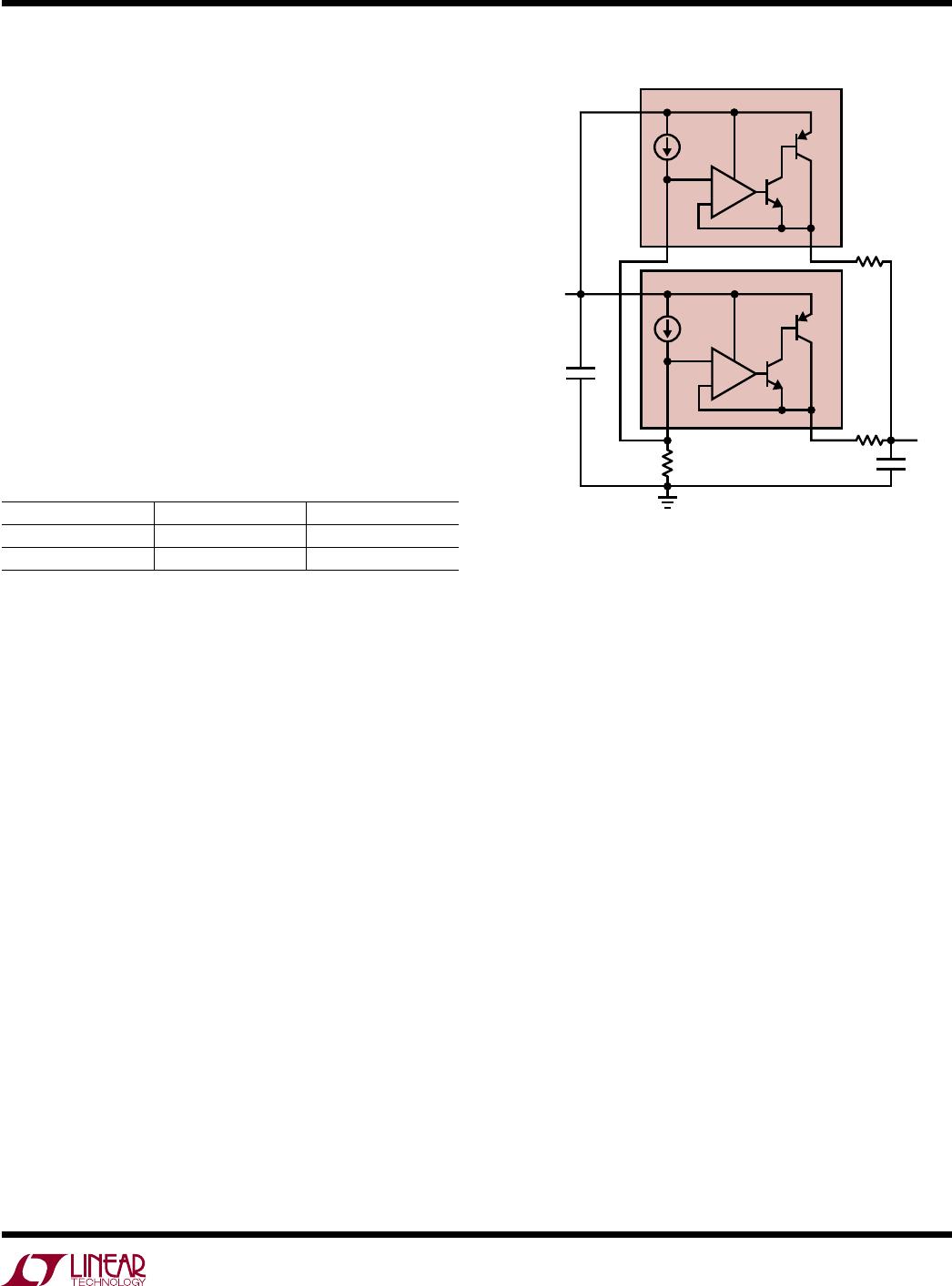
Load Voltage Regulation
The LT3081 is a floating device. No ground pin exists on
the packages. Thus, the IC delivers all quiescent current
and drive current to the load. Therefore, it is not possible
to provide true remote load sensing. The connection re
-
sistance between
the regulator and the load determines
load regulation performance. The data sheets load
regulation specification is Kelvin sensed at the package’s
pins. Negative-side sensing is a true Kelvin connection by
returning the bottom of the voltage setting resistor to the
negative side of the load (see Figure 10).
Connected as shown, system load regulation is the sum
of the LT3081’s load regulation and the parasitic line
resistance multiplied by the output current. To minimize
load regulation, keep the positive connection between the
regulator and load as short as possible. If possible, use
large diameter wire or wide PC board traces.
TEMP Pin Operation (Die Temperature Monitor)
The TEMP pin of the LT3081 outputs a current proportional
to average die temperature. At 25°C, the current from the
TEMP pin is 25µA, with a slope
ofA/°C. The current out
of the TEMP pin is valid for junction temperatures above
0°C (absent initial offset considerations). BelowC, the
TEMP pin will not sink current to indicate die temperature.
The TEMP pin output current is valid for voltages up to
40V below and 0.4V above the OUT pin allowing operation
even during short-circuit conditions.
Connecting a resistor from TEMP to ground converts the
TEMP pin current into a voltage to allow for monitoring
by an ADC. With a 1k resistor, 0mV to 150mV indicates
0°C to 150°C.
It should be noted that the TEMP pin current represents an
average temperature and should not be used to guarantee
that maximum junction temperature is not exceeded.
Instantaneous power along with thermal gradients and
time constants may cause portions of the die to exceed
maximum ratings and thermal shutdown thresholds. Be
sure to calculate die temperature rise for steady state (>1
minute) as well as impulse conditions.
I
MON
Pin Operation (Current Monitor)
The LT3081’s I
MON
pin outputs a current proportional to
the load current supplied at a ratio of 1:5000. The I
MON
pin current is valid for voltages up to 40V below and 0.4V
above
the OUT pin, allowing operation even during short-
cir
cuit conditions.
applicaTions inForMaTion
Figure 10. Connections for Best Load Regulation
IN
SET
+
LT3081
50µA
3081 F10
OUT
R
SET
R
P
PARASITIC
RESISTANCE
R
P
R
P
LOAD

LT3081IR#PBF

Mfr. #:
Manufacturer:
Analog Devices / Linear Technology
Description:
LDO Voltage Regulators 1.5A Single Resistor Programmable Rugged Linear Regulator
Lifecycle:
New from this manufacturer.
Delivery:
DHL FedEx Ups TNT EMS
Payment:
T/T Paypal Visa MoneyGram Western Union