LT3008 Series
13
3008fc
APPLICATIONS INFORMATION
DC BIAS VOLTAGE (V)
CHANGE IN VALUE (%)
3008 F03
20
0
–20
–40
–60
–80
–100
0
4
8
10
26
12
14
X5R
Y5V
16
BOTH CAPACITORS ARE 16V,
1210 CASE SIZE, 10µF
TEMPERATURE (°C)
–50
40
20
0
–20
–40
–60
–80
–100
25 75
3008 F04
–25 0
50 100 125
Y5V
CHANGE IN VALUE (%)
X5R
BOTH CAPACITORS ARE 16V,
1210 CASE SIZE, 10µF
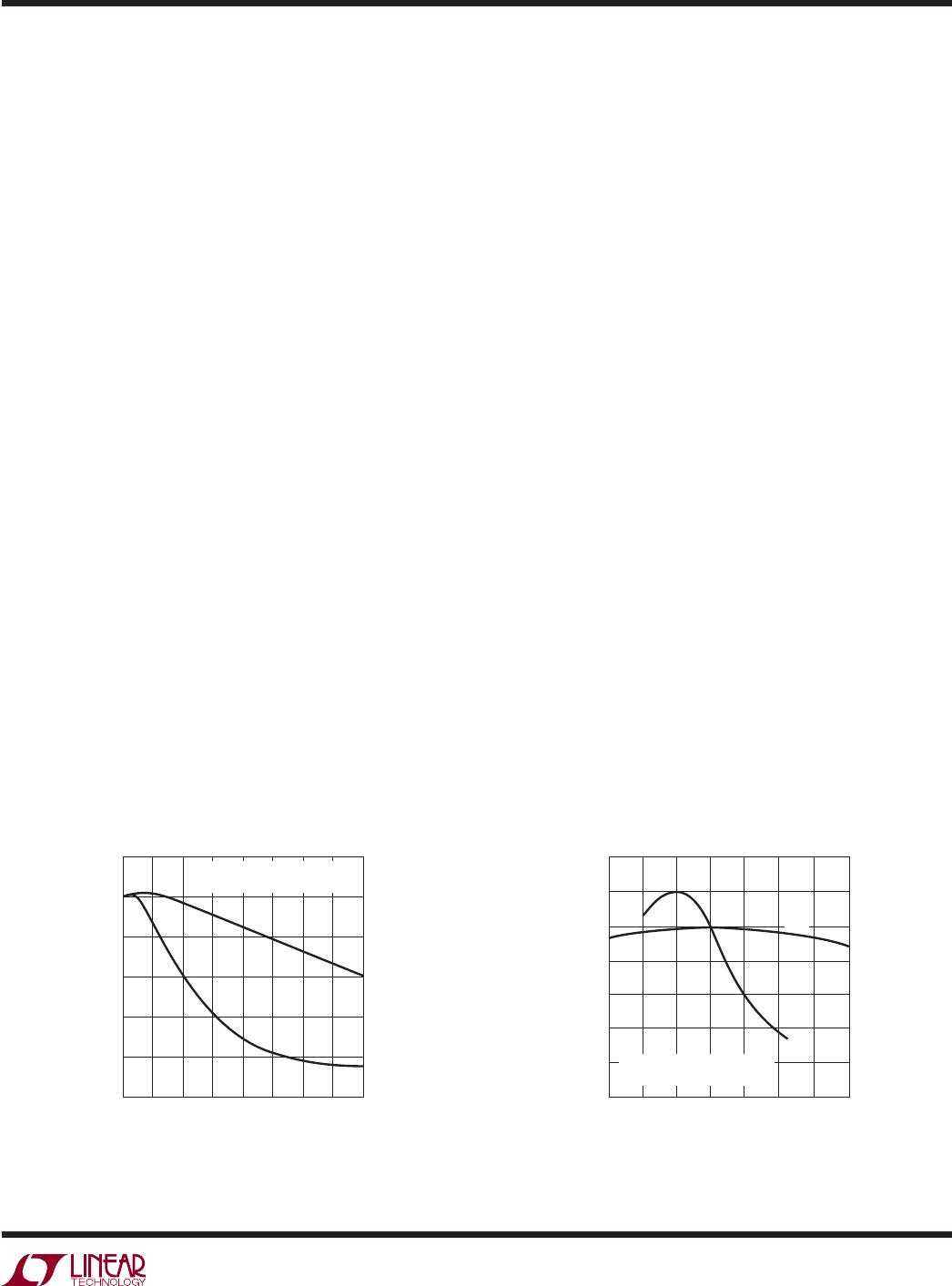
Figure 3. Ceramic Capacitor DC Bias Characteristics
Figure 4. Ceramic Capacitor Temperature Characteristics
Because the ADJ pin is relatively high impedance (de-
pending on the resistor divider used), stray capacitances
at this pin should be minimized. Special attention should
be given to any stray capacitances that can couple ex-
ternal signals onto the ADJ pin, producing undesirable
output transients or ripple.
Extra care should be taken in assembly when using high
valued resistors. Small amounts of board contamination
can lead to signifi cant shifts in output voltage. Appropriate
post-assembly board cleaning measures should be
implemented to prevent board contamination. If the
board is to be subjected to humidity cycling or if board
cleaning measures cannot be guaranteed, consideration
should be given to using resistors an order of magnitude
smaller than in Table 1 to prevent contamination from
causing unwanted shifts in the output voltage. A fi xed
voltage option in the LT3008 series will not need these
special considerations.
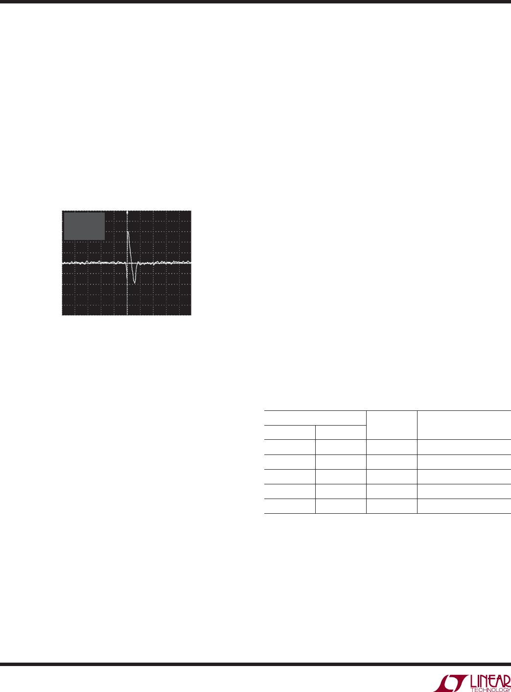
Output Capacitance and Transient Response
The LT3008 is stable with a wide range of output capacitors.
The ESR of the output capacitor affects stability, most
notably with small capacitors. Use a minimum output
capacitor of 2.2µF with an ESR of 3 or less to prevent
oscillations. The LT3008 is a micropower device and output
load transient response is a function of output capacitance.
Larger values of output capacitance decrease the peak
deviations and provide improved transient response for
larger load current changes.
Give extra consideration to the use of ceramic capacitors.
Manufacturers make ceramic capacitors with a variety of
dielectrics, each with different behavior across temperature
and applied voltage. The most common dielectrics are
specifi ed with EIA temperature characteristic codes of
Z5U, Y5V, X5R and X7R. The Z5U and Y5V dielectrics
provide high C-V products in a small package at low cost,
but exhibit strong voltage and temperature coeffi cients as
shown in Figures 3 and 4. When used with a 5V regulator,
a 16V 10µF Y5V capacitor can exhibit an effective value
as low as 1µF to 2µF for the DC bias voltage applied and
over the operating temperature range. The X5R and
X7R dielectrics yield more stable characteristics and are
more suitable for use as the output capacitor. The X7R
type has better stability across temperature, while the
X5R is less expensive and is available in higher values.
One must still exercise care when using X5R and X7R
capacitors; the X5R and X7R codes only specify operating
temperature range and maximum capacitance change
over temperature. Capacitance change due to DC bias
with X5R and X7R capacitors is better than Y5V and Z5U
capacitors, but can still be signifi cant enough to drop
capacitor values below appropriate levels. Capacitor DC
bias characteristics tend to improve as component case
size increases, but expected capacitance at operating
voltage should be verifi ed.
Voltage and temperature coeffi cients are not the only
sources of problems. Some ceramic capacitors have a
LT3008 Series
14
3008fc
APPLICATIONS INFORMATION
Figure 5. Noise Resulting from Tapping
on a Ceramic Capacitor
GND pin current is found by examining the GND Pin
Current curves in the Typical Performance Characteristics
section. Power dissipation is equal to the sum of the two
components listed prior.
The LT3008 regulator has internal thermal limiting designed
to protect the device during overload conditions. For
continuous normal conditions, do not exceed the maximum
junction temperature rating of 125°C. Carefully consider
all sources of thermal resistance from junction to ambient
including other heat sources mounted in proximity to
the LT3008. For surface mount devices, heat sinking is
accomplished by using the heat spreading capabilities of
the PC board and its copper traces. Copper board stiffeners
and plated through-holes can also be used to spread the
heat generated by power devices.
The following tables list thermal resistance for several
different board sizes and copper areas. All measurements
were taken in still air on 3/32" FR-4 two-layer boards with
one ounce copper.
PCB layers, copper weight, board layout and thermal vias
affect the resultant thermal resistance. Although Tables
2 and 3 provide thermal resistance numbers for 2-layer
boards with 1 ounce copper, modern multilayer PCBs
provide better performance than found in these tables.
100ms/DIV
V
OUT
500µV/DIV
3008 F0
5
V
OUT
= 0.6V
C
OUT
= 22µF
I
LOAD
= 10µA
piezoelectric response. A piezoelectric device generates
voltage across its terminals due to mechanical stress,
similar to the way a piezoelectric accelerometer or
microphone works. For a ceramic capacitor, the stress
can be induced by vibrations in the system or thermal
transients. The resulting voltages produced can cause
appreciable amounts of noise, especially when a ceramic
capacitor is used for noise bypassing. A ceramic capacitor
produced Figure 5’s trace in response to light tapping from a
pencil. Similar vibration induced behavior can masquerade
as increased output voltage noise.
Table 2: Measured Thermal Resistance for DC Package
COPPER AREA
BOARD
AREA
THERMAL RESISTANCE
(JUNCTION-TO-AMBIENT)TOPSIDE* BACKSIDE
2500mm
2
2500mm
2
2500mm
2
65°C/W
1000mm
2
2500mm
2
2500mm
2
70°C/W
225mm
2
2500mm
2
2500mm
2
75°C/W
100mm
2
2500mm
2
2500mm
2
80°C/W
50mm
2
2500mm
2
2500mm
2
85°C/W
*Device is mounted on the topside.
Thermal Considerations
The LT3008’s maximum rated junction temperature of
125°C limits its power-handling capability. Two components
comprise the power dissipated by the device:
1. Output current multiplied by the input/output voltage
differential: I
OUT
• (V
IN
– V
OUT
)
2. GND pin current multiplied by the input voltage:
I
GND
• V
IN
LT3008 Series
15
3008fc
APPLICATIONS INFORMATION
So,
P = 20mA(12.6V – 3.3V) + 0.3mA(12.6V) = 189.8mW
The thermal resistance ranges from 65°C/W to 85°C/W
depending on the copper area. So, the junction temperature
rise above ambient approximately equals:
0.1898W(75°C/W) = 14.2°C
The maximum junction temperature equals the maximum
junction temperature rise above ambient plus the maximum
ambient temperature or:
T
J(MAX)
= 85°C + 14.2°C = 99.2°C
Protection Features
The LT3008 incorporates several protection features that
make it ideal for use in battery-powered circuits. In ad-
dition to the normal protection features associated with
monolithic regulators, such as current limiting and thermal
limiting, the device also protects against reverse-input
voltages, reverse-output voltages and reverse output-to-
input voltages.
Current limit protection and thermal overload protec-
tion protect the device against current overload condi-
tions at the output of the device. For normal operation,
do not exceed a junction temperature of 125°C. The
typical thermal shutdown circuitry temperature threshold
is 160°C.
The IN pin withstands reverse voltages of 50V. The device
limits current fl ow to less than 30µA (typically less than
1µA) and no negative voltage appears at OUT. The device
protects both itself and the load against batteries that are
plugged in backwards.
For example, a 4-layer, 1 ounce copper PCB board with
3 thermal vias from the DFN exposed backside or the
3 fused TSOT-23 GND pins to inner layer GND planes
achieves 45°C/W thermal resistance. Demo circuit DC
1388As board layout achieves this 45°C/W performance.
This is approximately a 30% improvement over the lowest
numbers shown in Tables 2 and 3.
Calculating Junction Temperature
Example: Given an output voltage of 3.3V, an input voltage
range of 12V ±5%, an output current range of 0mA to 20mA
and a maximum ambient temperature of 85°C, what will
the maximum junction temperature be for an application
using the DC package?
The power dissipated by the device is equal to:
I
OUT(MAX)
(V
IN(MAX)
– V
OUT
) + I
GND
(V
IN(MAX)
)
where,
I
OUT(MAX)
= 20mA
V
IN(MAX)
= 12.6V
I
GND
at (I
OUT
= 20mA, V
IN
= 12.6V) = 0.3mA
Table 3: Measured Thermal Resistance for TSOT-23 Package
COPPER AREA
BOARD
AREA
THERMAL RESISTANCE
(JUNCTION-TO-AMBIENT)TOPSIDE* BACKSIDE
2500mm
2
2500mm
2
2500mm
2
65°C/W
1000mm
2
2500mm
2
2500mm
2
67°C/W
225mm
2
2500mm
2
2500mm
2
70°C/W
100mm
2
2500mm
2
2500mm
2
75°C/W
50mm
2
2500mm
2
2500mm
2
85°C/W
*Device is mounted on the topside.

LT3008EDC#TRMPBF

Mfr. #:
Manufacturer:
Analog Devices / Linear Technology
Description:
LDO Voltage Regulators 3uA Iq, 20mA Low Dropout Linear Regulators
Lifecycle:
New from this manufacturer.
Delivery:
DHL FedEx Ups TNT EMS
Payment:
T/T Paypal Visa MoneyGram Western Union