LT3008 Series
16
3008fc
APPLICATIONS INFORMATION
The SHDN pin cannot be driven below GND unless tied to
the IN pin. If the SHDN pin is driven below GND while IN
is powered, the output will turn on. SHDN pin logic cannot
be referenced to a negative rail.
The LT3008 incurs no damage if OUT is pulled below
ground. If IN is left open circuit or grounded, OUT can be
pulled below ground by 50V. No current fl ows from the
pass transistor connected to OUT. However, current fl ows
in (but is limited by) the resistor divider that sets output
voltage. Current fl ows from the bottom resistor in the
divider and from the ADJ pin’s internal clamp through the
top resistor in the divider to the external circuitry pulling
OUT below ground. If IN is powered by a voltage source,
OUT sources current equal to its current limit capability and
the LT3008 protects itself by thermal limiting if necessary.
In this case, grounding the SHDN pin turns off the LT3008
and stops OUT from sourcing current.
The LT3008 incurs no damage if the ADJ pin is pulled
above or below ground by 50V. If IN is left open circuit or
grounded, ADJ acts like a 100k resistor in series with a
diode when pulled above or below ground.
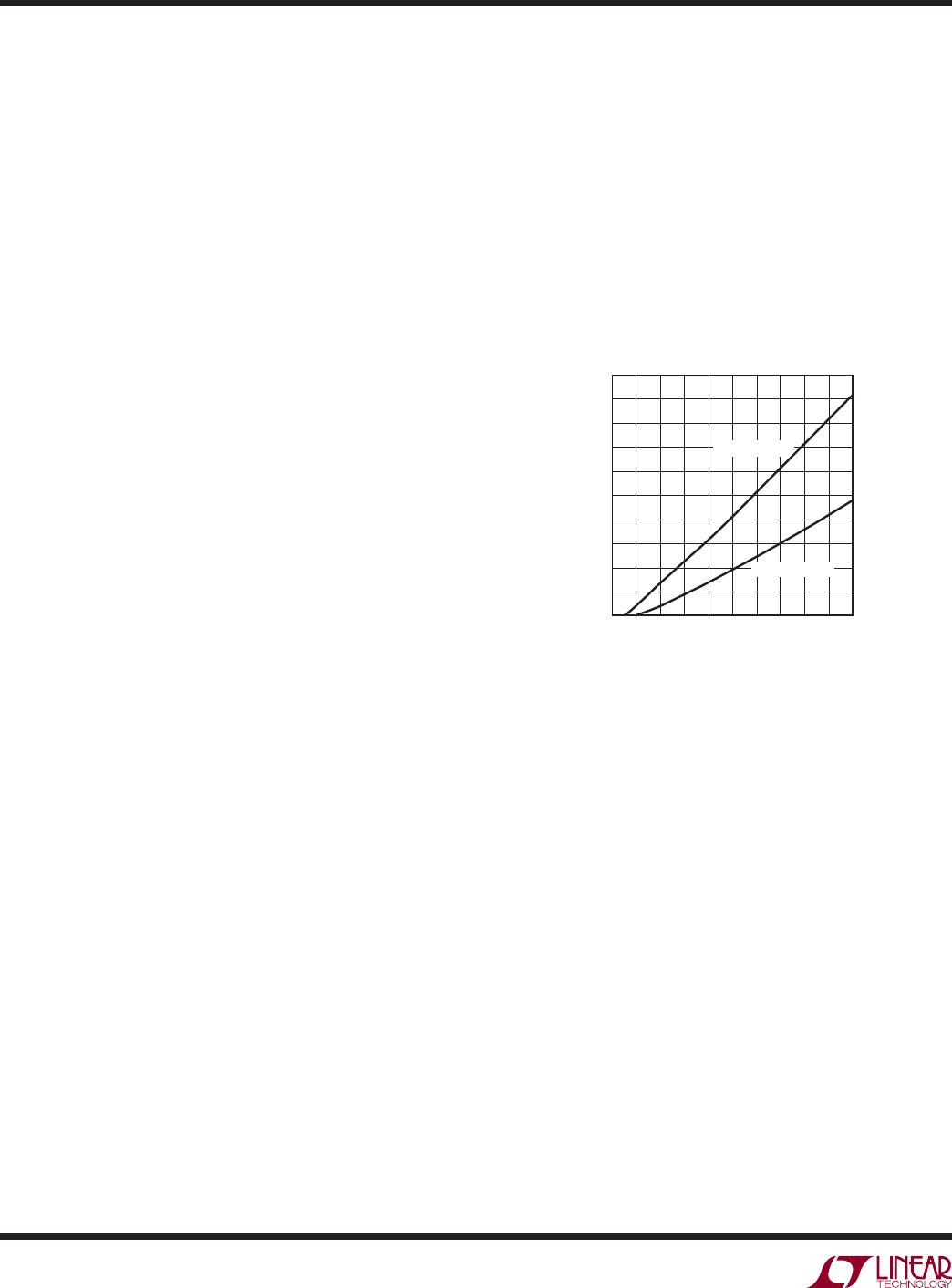
In circuits where a backup battery is required, several
different input/output conditions can occur. The output
voltage may be held up while the input is either pulled
OUTPUT AND ADJ VOLTAGE (V)
0
60
80
100
8
40
20
50
70
90
30
10
0
21
43
67 9
5
10
3008 F06
REVERSE CURRENT (µA)
OUT CURRENT
ADJ CURRENT
Figure 6. Reverse-Output Current
to ground, pulled to some intermediate voltage or is left
open circuit. Current fl ow back into the output follows the
curve shown in Figure 6.
If the LT3008 IN pin is forced below the OUT pin or the
OUT pin is pulled above the IN pin, input current typically
drops to less than 1µA. This occurs if the LT3008 input is
connected to a discharged (low voltage) battery and either
a backup battery or a second regulator circuit holds up
the output. The state of the SHDN pin has no effect in the
reverse current if OUT is pulled above IN.
LT3008 Series
17
3008fc
TYPICAL APPLICATIONS
IN
SHDN
3.3V
3009 TA02
OUT
F
2.2µF
SENSE
GND
L
T3008-3.3
NO PROTECTION
DIODES NEEDED!
V
IN
12V
LOAD:
SYSTEM MONITOR,
VOLATILE MEMORY, ETC.
IN
SHDN
5V
3008 TA03
OUT
FAULT
F
SUPERCAP 2.2µF
SENSE
PWR
TO
MONITORING
CENTER
SENSE
GND
GND
L
T3008-5
LINE POWER
V
LINE
12V TO 15V
D
CHARGE
R
LIMIT
LINE
INTERRUPT
DETECT
Keep-Alive Power Supply
Last-Gasp Circuit
PACKAGE DESCRIPTION
NOTE:
1. DRAWING TO BE MADE A JEDEC PACKAGE OUTLINE M0-229 VARIATION OF (WCCD-2)
2. DRAWING NOT TO SCALE
3. ALL DIMENSIONS ARE IN MILLIMETERS
4. DIMENSIONS OF EXPOSED PAD ON BOTTOM OF PACKAGE DO NOT INCLUDE
MOLD FLASH. MOLD FLASH, IF PRESENT, SHALL NOT EXCEED 0.15mm ON ANY SIDE
2.00 ±0.10
(4 SIDES)
0.75 ±0.05
PIN 1 BAR
TOP MARK
(SEE NOTE 6)
0.200 REF
0.00 – 0.05
0.25 ±0.05
1.42 ±0.05
(2 SIDES)
RECOMMENDED SOLDER PAD PITCH AND DIMENSIONS
0.61 ±0.05
(2 SIDES)
1.15 ±0.05
0.70 ±0.05
2.55 ±0.05
PACKAGE
OUTLINE
0.50 BSC
0.40 ±0.10
BOTTOM VIEW—EXPOSED PAD
0.56 ±0.05
(2 SIDES)
R = 0.125
TYP
R = 0.05
TYP
1.37 ±0.05
(2 SIDES)
1
3
64
(DC6) DFN REV B 1309
0.25 ±0.05
0.50 BSC
PIN 1 NOTCH
R = 0.20 OR
0.25 × 45°
CHAMFER
5. EXPOSED PAD SHALL BE SOLDER PLATED
6. SHADED AREA IS ONLY A REFERENCE FOR PIN 1 LOCATION ON THE
TOP AND BOTTOM OF PACKAGE
DC6 Package
6-Lead Plastic DFN (2mm × 2mm)
(Reference LTC DWG # 05-08-1703 Rev B)
LT3008 Series
18
3008fc
1.50 – 1.75
(NOTE 4)
2.80 BSC
0.22 – 0.36
8 PLCS (NOTE 3)
DATUM ‘A
0.09 – 0.20
(NOTE 3)
TS8 TSOT-23 0710 REV A
2.90 BSC
(NOTE 4)
0.65 BSC
1.95 BSC
0.80 – 0.90
1.00 MAX
0.01 – 0.10
0.20 BSC
0.30 – 0.50 REF
PIN ONE ID
NOTE:
1. DIMENSIONS ARE IN MILLIMETERS
2. DRAWING NOT TO SCALE
3. DIMENSIONS ARE INCLUSIVE OF PLATING
4. DIMENSIONS ARE EXCLUSIVE OF MOLD FLASH AND METAL BURR
5. MOLD FLASH SHALL NOT EXCEED 0.254mm
6. JEDEC PACKAGE REFERENCE IS MO-193
3.85 MAX
0.40
MAX
0.65
REF
RECOMMENDED SOLDER PAD LAYOUT
PER IPC CALCULATOR
1.4 MIN
2.62 REF
1.22 REF
TS8 Package
8-Lead Plastic TSOT-23
(Reference LTC DWG # 05-08-1637 Rev A)
PACKAGE DESCRIPTION

LT3008EDC#TRMPBF

Mfr. #:
Manufacturer:
Analog Devices / Linear Technology
Description:
LDO Voltage Regulators 3uA Iq, 20mA Low Dropout Linear Regulators
Lifecycle:
New from this manufacturer.
Delivery:
DHL FedEx Ups TNT EMS
Payment:
T/T Paypal Visa MoneyGram Western Union