TDA7439 I
2
C bus transmission examples
13/23
5 I
2
C bus transmission examples
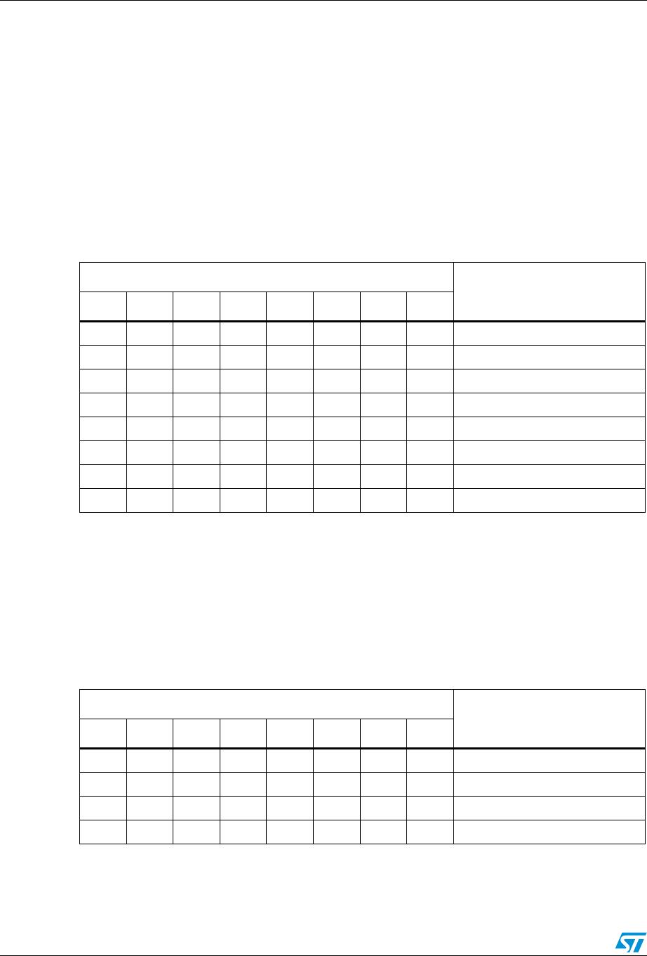
5.1 No address incrementing
The TDA7439 receives a start condition followed by the correct chip address, then a sub
address with the bit B = 0 (for no address increment), then the data bytes to be sent to the
sub address and finally a stop condition.
Figure 16. SDA addressing and data for B = 0
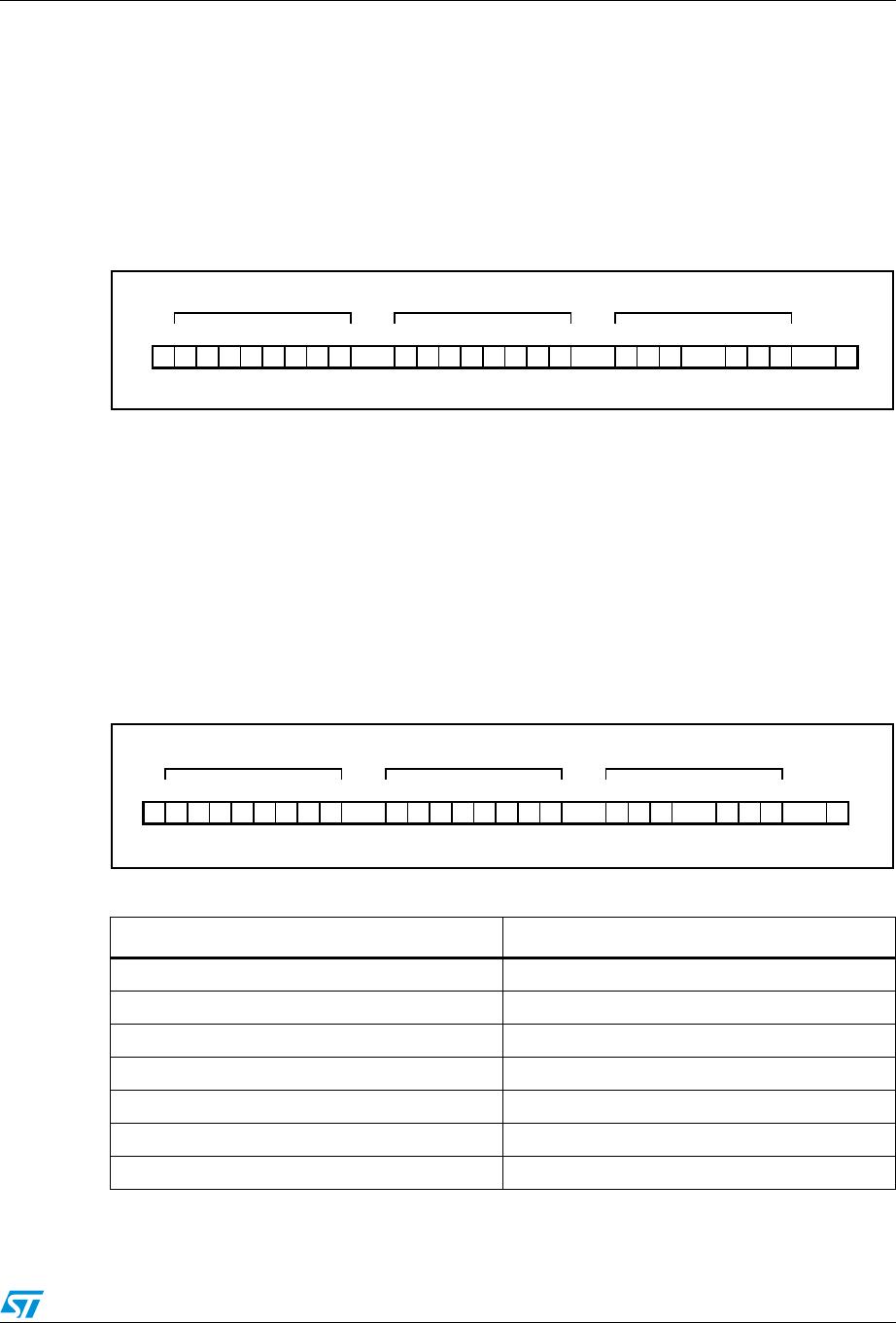
5.2 Address incrementing
The TDA7439 receives a start condition followed by the correct chip address, then a sub
address with the B = 1 for address incrementing; now it is in a loop condition with an
automatic increase of the sub address up to D[3:0] = 0x7. That is, the data for sub
addresses from D[3:0] = 1000 (binary) to 1111 are ignored.
In Figure 17 below, DATA1 is directed to the sub address sent (that is, D[3:0]), DATA2 is
directed to the sub address incremented by 1 (that is, 1 + D[3:0]) and so forth until a stop
condition is received to terminate the transmission.
Figure 17. SDA addressing and data for B = 1
S 1 0 0 0 1 0 0 0 ACK ACK DATA ACK P
MSB
LSB MSB LSB MSB LSB
CHIP ADDRESS
D96AU421
X
D3
SUBADDRESS DATA
X
X
0
D2 D1 D0
Table 6. Power-on-reset conditions
Parameter POR value
Input selection IN2
Input gain 28 dB
Volume MUTE
Bass 0 dB
Mid-range 2 dB
Tr ebl e 2 d B
Speaker MUTE
S 1 0 0 0 1 0 0 0 ACK ACK DATA ACK P
MSB
LSB MSB LSB MSB LSB
CHIP ADDRESS
D96AU422
X
D3
SUBADDRESS DATA 1 to DATA n
X
X
1
D2 D1 D0
Obsolete Product(s) - Obsolete Product(s)
I
2
C bus addresses and data TDA7439
14/23
6 I
2
C bus addresses and data
6.1 Chip address byte
The TDA7439 chip address is 0x88.
6.2 Sub-address byte
The function is selected by the 4-bit sub address as given in Table 7 . The three MSBs are
not used and bit D4 selects address incrementing (B = 1) or single data byte (B = 0).
6.3 Data bytes
The function value is changed by the data byte as given in the following tables, Tabl e 8 to
Table 14.
In the tables of input gain, volume and attenuation, not all values are shown. A desired
intermediate value is obtained by setting the three LSBs to the appropriate value.
Table 7. Function selection: sub-address byte
MSB LSB
Function
D7 D6 D5 D4 D3 D2 D1 D0
X X X B 0 0 0 0 Input selector
X X X B 0 0 0 1 Input gain
XXXB001 0Volume
XXXB001 1Bass gain
X X X B 0 1 0 0 Mid-range gain
XXXB010 1Treble gain
X X X B 0 1 1 0 Speaker attenuation, R
X X X B 0 1 1 1 Speaker attenuation, L
Table 8. Input selector value (sub address 0x0)
MSB LSB
Input multiplexer
D7 D6 D5 D4 D3 D2 D1 D0
XXXXXX00 IN4
XXXXXX01 IN3
XXXXXX10 IN2
XXXXXX11 IN1
Obsolete Product(s) - Obsolete Product(s)
TDA7439 I
2
C bus addresses and data
15/23
Table 9. Input gain value (sub address 0x1)
MSB LSB
Input gain
2-dB steps
D7 D6 D5 D4 D3 D2 D1 D0
XXXX000 0 0dB
XXXX000 1 2dB
XXXX001 0 4dB
XXXX001 1 6 dB
XXXX010 0 8dB
XXXX010 1 10dB
XXXX011 0 12dB
XXXX011 1 14dB
XXXX100 0 16dB
XXXX100 1 18dB
XXXX101 0 20dB
XXXX101 1 22dB
XXXX110 0 24dB
XXXX110 1 26dB
XXXX111 0 28dB
XXXX111 1 30dB
Table 10. Volume value (sub address 0x2)
MSB LSB
Volume
1-dB steps
D7 D6 D5 D4 D3 D2 D1 D0
X0000000 0dB
X0000001 -1dB
X0000010 -2dB
X0000011 -3dB
X0000100 -4dB
X0000101 -5dB
X0000110 -6dB
X0000111 -7dB
X0001000 -8dB
X0010000 -16dB
X0011000 -24dB
X0100000 -32dB
X0101000 -40dB
XX111XXX MUTE
Obsolete Product(s) - Obsolete Product(s)

TDA7439

Mfr. #:
Manufacturer:
STMicroelectronics
Description:
Audio DSPs 3-Band Digital Cont
Lifecycle:
New from this manufacturer.
Delivery:
DHL FedEx Ups TNT EMS
Payment:
T/T Paypal Visa MoneyGram Western Union

Products related to this Datasheet