TDA7439 Electrical specifications
7/23
Figure 3. Test circuit
0/30dB
2dB STEP
MUXOUTL INL
VOLUME
VOLUME
TREBLE
TREBLE
TREBLE(L)
MIDDLE
MIDDLE
MUXOUTR
INR TREBLE(R)
BOUT(L)
MIN(L)
SPKR ATT
LEFT
LOUT
SCL
SDA
DIGGND
ROUT
D95AU339B
I
2
CBUS DECODER + LATCHES
5.6nF
2.2µF
100K
100K
100K
100K
G
L-IN1
L-IN2
L-IN3
L-IN4
0.47µF
0.47µF
0.47µF
0.47µF
100K
100K
100K
100K
R-IN1
R-IN2
R-IN3
R-IN4
0.47µF
0.47µF
0.47µF
0.47µF
G
INPUT MULTIPLEXER
+ GAIN
MOUT(L)
BASS
BIN(L)
18nF 22nF 100nF 100nF
2.7K 5.6K
BASS
SPKR ATT
RIGHT
MIN(R)
MOUT(R) BOUT(R)BIN(R)
5.6nF
18nF 22nF 100nF 100nF
2.7K 5.6K
SUPPLY
10µF
CREF
AGND
V
S
R
M
R
B
R
M
R
B
6
11
12
13
14
10
9
8
7
30
1
29
5
3
4
17 18 28 19 20 21 22 2
15 16 27 26 25 23 24
V
REF
2.2µF
Obsolete Product(s) - Obsolete Product(s)
Application suggestions TDA7439
8/23
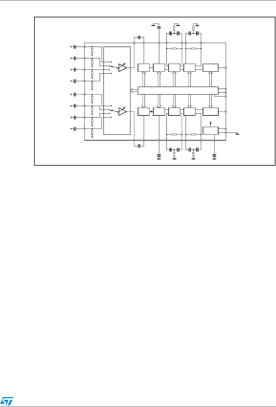
3 Application suggestions
The first and the last stages are volume control blocks. The control range is 0 to -47 dB and
mute for the first stage and 0 to -79 dB and mute for the last one. Both control blocks have a
step resolution of 1 dB.
This very high resolution allows the implementation of systems free from any noisy
acoustical effect.
The TDA7439 audio processor provides 3 bands of tone control (bass, mid-range and
treble).
3.1 Tone control
3.1.1 Bass, mid-range stages
The bass and the mid-range cells have the same structure.
However, the bass cell has an internal resistor R
B
of typically 44 k whilst the mid-range cell
has an internal resistor R
M
of typically 25 k.
Several filter types can be implemented by connecting external components to the bass/mid
IN and OUT pins.
Typical responses are shown in Figure 8, Figure 9 and Figure 11.
Figure 4. Bass/mid-range filter implementation
Figure 4. refers to the basic T-type band-pass filter. Starting from the filter component values
(R1 (internal) and R2, C1, C2 (external)) then the centre frequency f
C
, the gain Av at
maximum boost and the filter Q factor are computed as follows:
Ri internal
C
2
OUTIN
C
1
R
2
D95AU313
f
C
1
2 π R1 R2 C1 C2⋅⋅⋅⋅⋅
-----------------------------------------------------------------=
A
V
R2C2 R2C1 RiC1++
R2C1 R2C2+
----------------------------------------------------------- -=
Q
R1 R2 C1 C2⋅⋅⋅
R2C1 R2C2+
-------------------------------------------------=
Obsolete Product(s) - Obsolete Product(s)
TDA7439 Application suggestions
9/23
Transposing and solving for the external component values we get:
3.1.2 Treble stage
The treble stage is a high-pass filter whose time constant is fixed by an internal resistor
(25 k typically) and an external capacitor connected between treble pins and ground.
Typical responses are shown in Figure 10 and Figure 11.
3.2 Pin CREF
The suggested value of 10 µF for the reference capacitor (C
REF
), connected to pin CREF,
can be reduced to 4.7 µF if the application requires faster power-on.
3.3 Electrical characteristics
C1
A
V
1
2 π Fc Ri Q⋅⋅
------------------------------------------=
C2
Q
2
C1
A
V
1 Q
2
----------------------------- -=
R2
A
V
1 Q
2
2 π C1 Fc A
V
1()Q⋅⋅⋅⋅
----------------------------------------------------------------------=
Figure 5. THD vs frequency Figure 6. THD vs R
LOAD
Obsolete Product(s) - Obsolete Product(s)

TDA7439

Mfr. #:
Manufacturer:
STMicroelectronics
Description:
Audio DSPs 3-Band Digital Cont
Lifecycle:
New from this manufacturer.
Delivery:
DHL FedEx Ups TNT EMS
Payment:
T/T Paypal Visa MoneyGram Western Union

Products related to this Datasheet