ICS854S01AKI REVISION A OCTOBER 29, 2012 7 ©2012 Integrated Device Technology, Inc.
ICS854S01I Data Sheet 2:1 DIFFERENTIAL-TO-LVDS MULTIPLEXER
Parameter Measurement Information, continued
Output Duty Cycle/Pulse Width/Period
Offset Voltage Setup
Differential Output Voltage Setup
t
PW
t
PERIOD
t
PW
t
PERIOD
odc = x 100%
Q
nQ
out
out
LVDS
DC Input
ä
V
OS
/Δ V
OS
V
DD
100
out
out
DC Input
V
DD
LVDS
ICS854S01AKI REVISION A OCTOBER 29, 2012 8 ©2012 Integrated Device Technology, Inc.
ICS854S01I Data Sheet 2:1 DIFFERENTIAL-TO-LVDS MULTIPLEXER
Application Information
Wiring the Differential Input to Accept Single Ended Levels
Figure 1 shows how the differential input can be wired to accept
single ended levels. The reference voltage V_REF = V
DD
/2 is
generated by the bias resistors R1, R2 and C1. This bias circuit
should be located as close as possible to the input pin. The ratio of
R1 and R2 might need to be adjusted to position the V_REF in the
center of the input voltage swing. For example, if the input clock swing
is only 2.5V and V
DD
= 3.3V, V_REF should be 1.25V and R2/R1 =
0.609.
Figure 1. Single-Ended Signal Driving Differential Input
Recommendations for Unused Input Pins
Inputs:
PCLK/nPCLK Inputs:
For applications not requiring the use of the differential input, both
PCLK and nPCLK can be left floating. Though not required, but for
additional protection, a 1k resistor can be tied from PCLK to
ground.
R2
1K
V
DD
CLK_IN
R1
1K
C1
0.1uF
V_REF
PCLKx
nPCLKx
ICS854S01AKI REVISION A OCTOBER 29, 2012 9 ©2012 Integrated Device Technology, Inc.
ICS854S01I Data Sheet 2:1 DIFFERENTIAL-TO-LVDS MULTIPLEXER
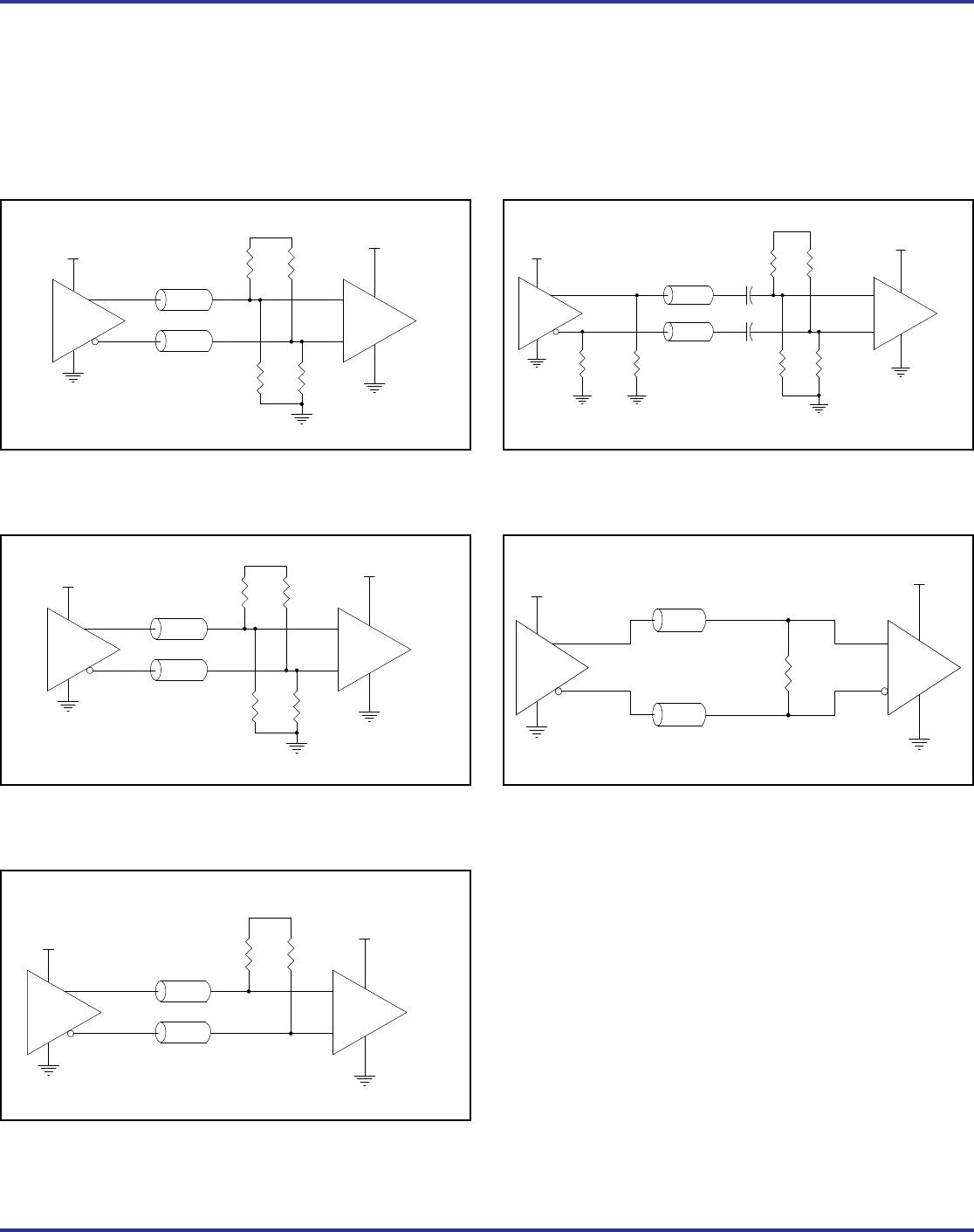
LVPECL Clock Input Interface
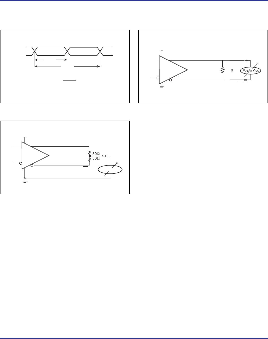
The PCLK /nPCLK accepts LVPECL, LVDS and other differential
signals. Both signals must meet the V
PP
and V
CMR
input
requirements. Figures 2A to 2C show interface examples for the
PCLK/ nPCLK input driven by the most common driver types. The
input interfaces suggested here are examples only. If the driver is
from another vendor, use their termination recommendation. Please
consult with the vendor of the driver component to confirm the driver
termination requirements.
Figure 2A. PCLK/nPCLK Input Driven by a
3.3V LVDS Driver
Figure 2C. PCLK/nPCLK Input Driven by a
3.3V LVPECL Driver
Figure 2E. PCLK/nPCLK Input Driven by a CML Driver
Figure 2B. PCLK/nPCLK Input Driven by a
3.3V LVPECL Driver with AC Couple
Figure 2D. PCLK/nPCLK Input Driven by a
Built-In Pullup CML Driver
R3
125Ω
R4
125Ω
R1
84Ω
R2
84Ω
3.3V
Zo = 50Ω
Zo = 50Ω
PCLK
nPCLK
3.3V
3.3V
LVPECL
LVPECL
Input
PCLK
nPCLK
LVPECL
Input
CML
3.3V
Zo = 50Ω
Zo = 50Ω
3.3V
3.3V
R1
50Ω
R2
50Ω
R3
84
R4
84
R1
125
R2
125
R5
100 - 200
R6
100 - 200
PCLK
nPCLK
3.3V LVPECL
3.3V
Zo = 50Ω
Zo = 50Ω
3.3V
3.3V
LVPECL
Input
C1
C2
PCLK
nPCLK
3.3V
LVPECL
Input
3.3V
Zo = 50Ω
Zo = 50Ω
R1
100Ω
CML Built-In Pullup

854S01AKILF

Mfr. #:
Manufacturer:
IDT
Description:
Clock Drivers & Distribution 2:1 Diff to LVDS Multplexer 2.5GHz
Lifecycle:
New from this manufacturer.
Delivery:
DHL FedEx Ups TNT EMS
Payment:
T/T Paypal Visa MoneyGram Western Union

Products related to this Datasheet