Integrated Silicon Solution, Inc. — www.issi.com 1
Rev. E
01/10/2013
Copyright © 2013 Integrated Silicon Solution, Inc. All rights reserved. ISSI reserves the right to make changes to this specification and its products at any time with-
out notice. ISSI assumes no liability arising out of the application or use of any information, products or services described herein. Customers are advised to obtain
the latest version of this device specification before relying on any published information and before placing orders for products.
IS61WV12816DALL/DALS
IS61WV12816DBLL/DBLS
IS64WV12816DBLL/DBLS
FEATURES
HIGH SPEED: (IS61/64WV12816DALL/DBLL)
• High-speedaccesstime:8,10,12,20ns
• LowActivePower:135mW(typical)
• LowStandbyPower:12µW(typical)
CMOS standby
LOW POWER: (IS61/64WV12816DALS/DBLS)
• High-speedaccesstime:25,35ns
• LowActivePower:55mW(typical)
• LowStandbyPower:12µW(typical)
CMOS standby
• Singlepowersupply
— Vdd1.65Vto2.2V(IS61WV12816DAxx)
— Vdd2.4Vto3.6V(IS61/64WV12816DBxx)
• Fullystaticoperation:noclockorrefresh
required
• Threestateoutputs
• Datacontrolforupperandlowerbytes
• IndustrialandAutomotivetemperaturesupport
• Lead-freeavailable
128K x 16 HIGH SPEED ASYNCHRONOUS
CMOS STATIC RAM
DESCRIPTION
TheISSIIS61WV12816DAxx/DBxxandIS64WV12816D-
Bxxarehigh-speed,2,097,152-bitstaticRAMsorganized
as131,072wordsby16bits.ItisfabricatedusingISSI's
high-performanceCMOStechnology.Thishighlyreliable
process coupled with innovative circuit design techniques,
yields high-performance and low power consumption
devices.
When CE is HIGH (deselected), the device assumes a
standby mode at which the power dissipation can be re-
duced down with CMOS input levels.
EasymemoryexpansionisprovidedbyusingChipEnable
andOutputEnableinputs,CEandOE.TheactiveLOW
Write Enable (WE) controls both writing and reading of the
memory. A data byte allows Upper Byte (UB) and Lower
Byte (LB) access.
The IS61WV12816DAxx/DBxx and IS64WV12816DBxx
arepackagedintheJEDECstandard44-pinTSOPType
IIand48-pinMiniBGA(6mmx8mm).
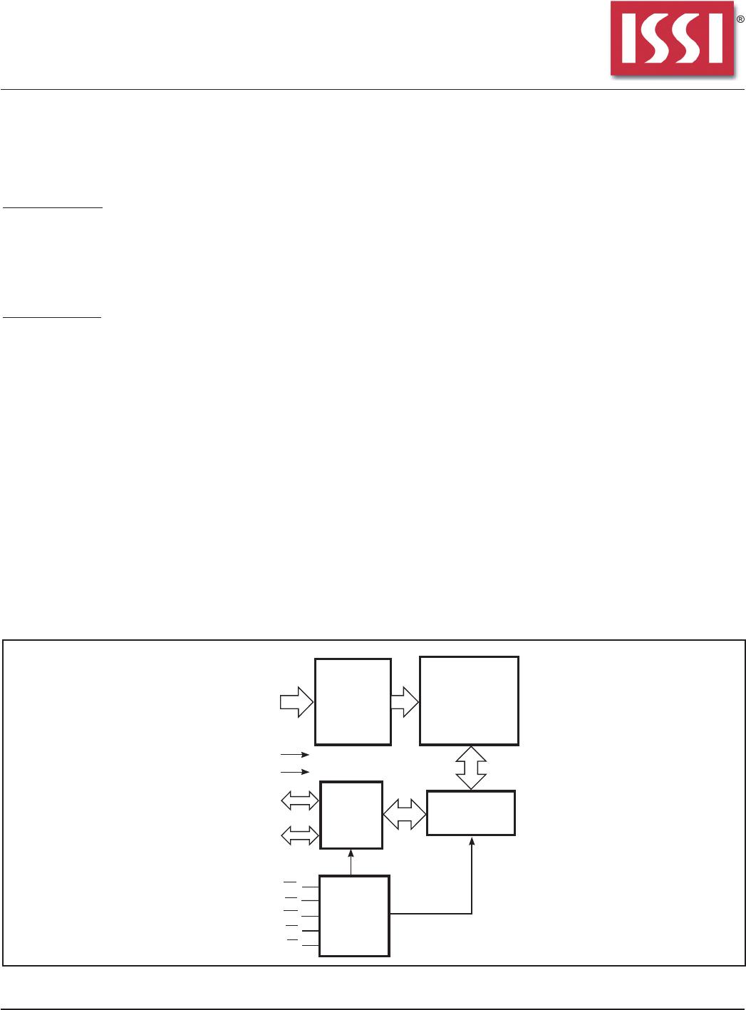
FUNCTIONAL BLOCK DIAGRAM
A0-A16
CE
OE
WE
128K x 16
MEMORY ARRAY
DECODER
COLUMN I/O
CONTROL
CIRCUIT
GND
VDD
I/O
DATA
CIRCUIT
I/O0-I/O7
Lower Byte
I/O8-I/O15
Upper Byte
UB
LB
JANUARY 2013

