IS64WV12816DBLL-12CTLA3-TR

10 Integrated Silicon Solution, Inc. — www.issi.com
Rev. E
01/10/2013
IS61WV12816DALL/DALS, IS61WV12816DBLL/DBLS,
IS64WV12816DBLL/DBLS
READ CYCLE SWITCHING CHARACTERISTICS
(1)
(Over Operating Range)
-20 ns -25 ns -35 ns -45 ns
Symbol Parameter Min. Max. Min. Max. Min. Max. Min. Max. Unit
trc ReadCycleTime 20 — 25 — 35 — 45 — ns
tAA AddressAccessTime — 20 — 25 — 35 — 45 ns
toHA OutputHoldTime 2.5 — 6 — 8 — 10 — ns
tAce CEAccessTime — 20 — 25 — 35 — 45 ns
tdoe OEAccessTime — 8 — 12 — 15 — 20 ns
tHzoe
(2)
OEtoHigh-ZOutput 0 8 0 8 0 10 0 15 ns
tLzoe
(2)
OE to Low-Z Output 0 0 0 0 ns
tHzce
(2
CEtoHigh-ZOutput 0 8 0 8 0 10 0 15 ns
tLzce
(2)
CE to Low-Z Output 3 10 10 10 ns
tbA LB, UBAccessTime — 8 — 25 — 35 — 45 ns
tHzb LB, UBtoHigh-ZOutput 0 8 0 8 0 10 0 15 ns
tLzb LB, UB to Low-Z Output 0 0 0 0 ns
Notes:
1. Testconditionsassumesignaltransitiontimesof1.5nsorless,timingreferencelevelsof1.25V,inputpulselevelsof0.4Vto
Vdd-0.3VandoutputloadingspeciedinFigure1a.
2. TestedwiththeloadinFigure1b.Transitionismeasured±500mVfromsteady-statevoltage.Not100%tested.
3. Not 100% tested.
Integrated Silicon Solution, Inc. — www.issi.com 11
Rev. E
01/10/2013
IS61WV12816DALL/DALS, IS61WV12816DBLL/DBLS,
IS64WV12816DBLL/DBLS
DATA VALID
READ1.eps
PREVIOUS DATA VALID
t
AA
t
OHA
t
OHA
t
RC
DOUT
ADDRESS
AC WAVEFORMS
READ CYCLE NO. 1
(1,2)
(Address Controlled) (CE = OE = VIL, UB or LB = VIL)
t
RC
t
OHA
t
AA
t
DOE
t
LZOE
t
ACE
t
LZCE
t
HZOE
HIGH-Z
DATA VALID
UB_CEDR2.eps
t
HZB
ADDRESS
OE
CE
LB, UB
D
OUT
t
HZCE
t
BA
t
LZB
t
RC
t
PD
I
SB
I
CC
50%
V
DD
Supply
Current
50%
t
PU
READ CYCLE NO. 2
(1,3)
Notes:
1. WE is HIGH for a Read Cycle.
2. Thedeviceiscontinuouslyselected.OE, CE, UB, or LB = VIL.
3. Address is valid prior to or coincident with CE LOW transition.
12 Integrated Silicon Solution, Inc. — www.issi.com
Rev. E
01/10/2013
IS61WV12816DALL/DALS, IS61WV12816DBLL/DBLS,
IS64WV12816DBLL/DBLS
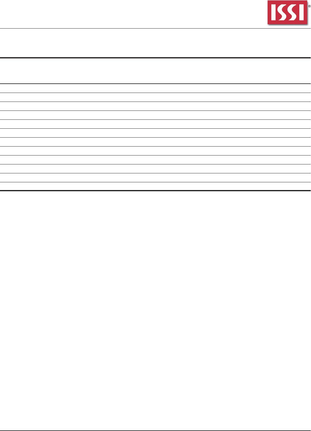
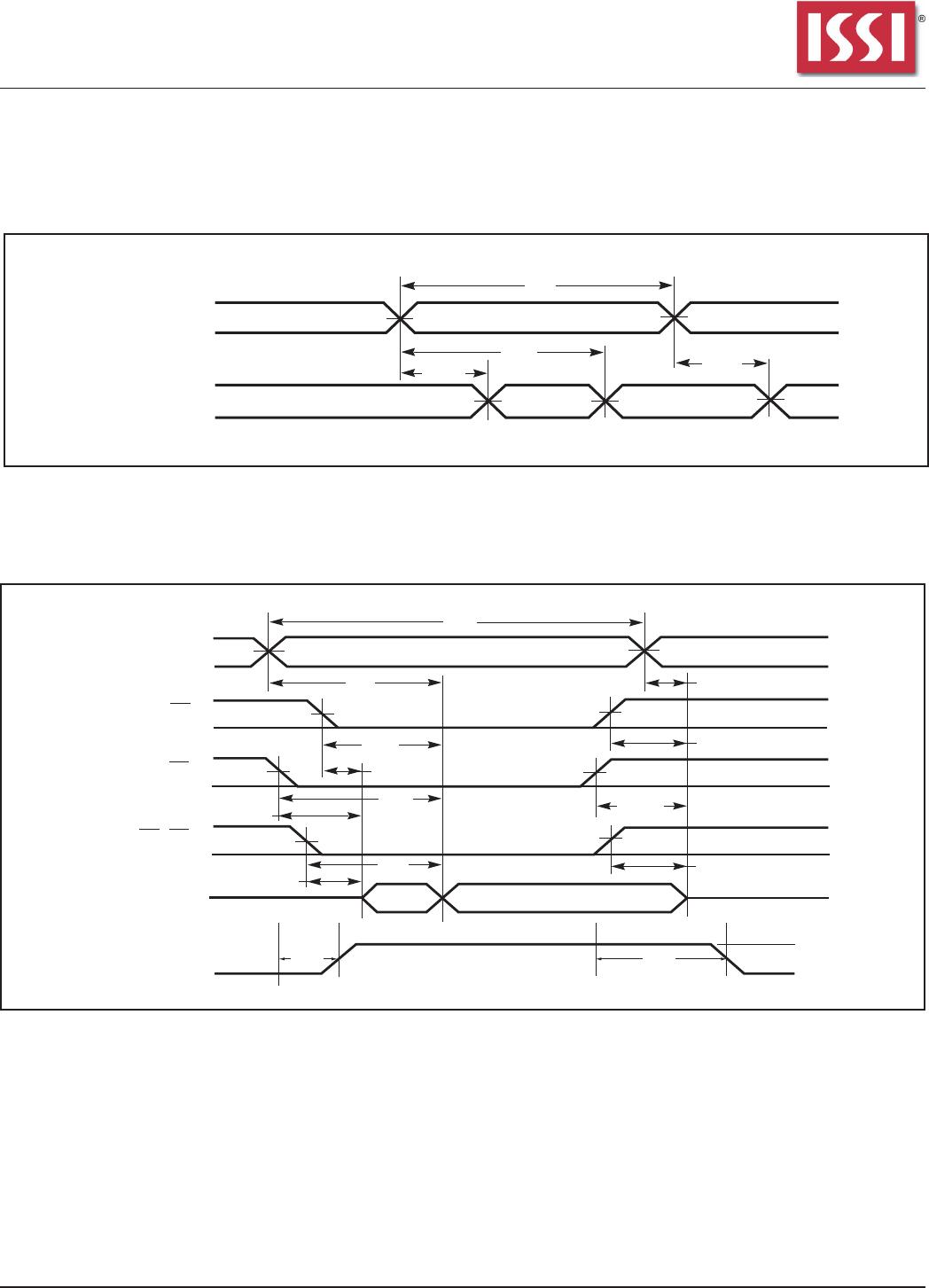
WRITE CYCLE SWITCHING CHARACTERISTICS
(1,3)
(Over Operating Range)
-8 -10 -12
Symbol Parameter Min. Max. Min. Max. Min. Max. Unit
twc WriteCycleTime 8 — 10 — 12 — ns
tsce CEtoWriteEnd 6.5 — 8 — 9 — ns
tAw AddressSetupTime 6.5 — 8 — 9 — ns
to Write End
tHA Address Hold from Write End 0 0 0 ns
tsA AddressSetupTime 0 — 0 — 0 — ns
tPwb LB, UBValidtoEndofWrite 6.5 — 8 — 9 — ns
tPwe1 WEPulseWidth 6.5 — 8 — 9 — ns
tPwe2 WE Pulse Width (OE = LOW) 8.0 10 11 ns
tsd DataSetuptoWriteEnd 5 — 6 — 9 — ns
tHd Data Hold from Write End 0 0 0 ns
tHzwe
(2)
WELOWtoHigh-ZOutput — 3.5 — 5 — 6 ns
tLzwe
(2)
WE HIGH to Low-Z Output 2 2 3 ns
Notes:
1. Testconditionsassumesignaltransitiontimesof3nsorless,timingreferencelevelsof1.5V,inputpulselevelsof0Vto3.0V
andoutputloadingspeciedinFigure1.
2. TestedwiththeloadinFigure2.Transitionismeasured±500mVfromsteady-statevoltage.Not100%tested.
3. TheinternalwritetimeisdenedbytheoverlapofCE LOW and UB or LB, and WE LOW. All signals must be in valid states
toinitiateaWrite,butanyonecangoinactivetoterminatetheWrite.TheDataInputSetupandHoldtimingarereferencedto
the rising or falling edge of the signal that terminates the write. Shaded area product in development

IS64WV12816DBLL-12CTLA3-TR

Mfr. #:
Manufacturer:
ISSI
Description:
SRAM 2M (128Kx16) 12ns Async SRAM
Lifecycle:
New from this manufacturer.
Delivery:
DHL FedEx Ups TNT EMS
Payment:
T/T Paypal Visa MoneyGram Western Union