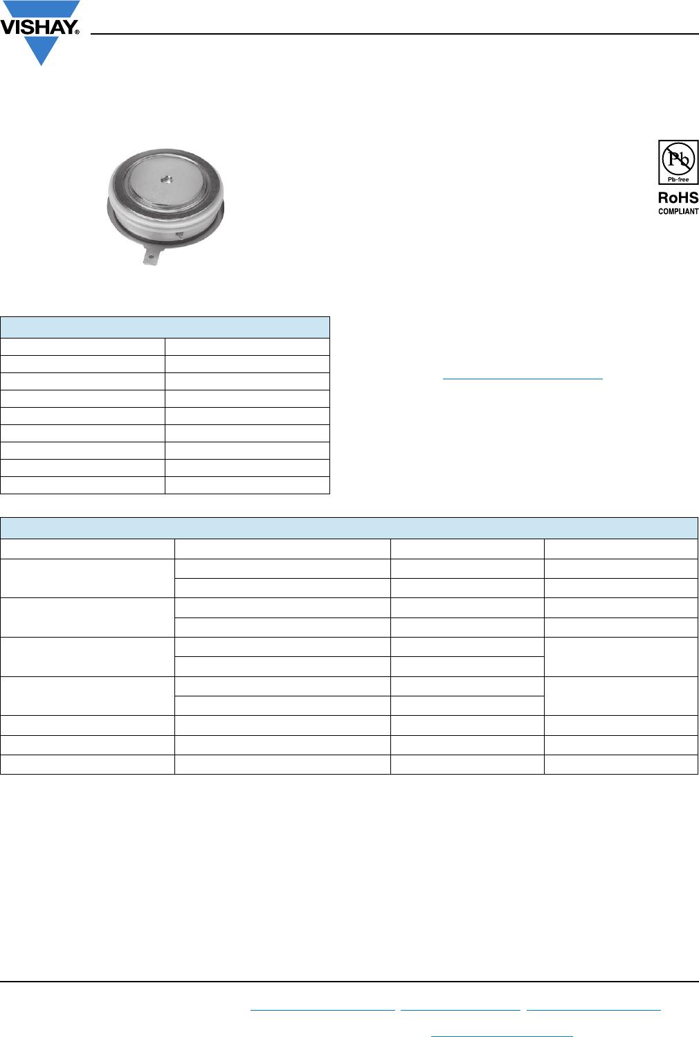
VS-ST303C12LFK0

VS-ST303C Series
www.vishay.com
Vishay Semiconductors
Revision: 20-Dec-13
1
Document Number: 94373
For technical questions within your region: DiodesAmericas@vishay.com
, DiodesAsia@vishay.com, DiodesEurope@vishay.com
THIS DOCUMENT IS SUBJECT TO CHANGE WITHOUT NOTICE. THE PRODUCTS DESCRIBED HEREIN AND THIS DOCUMENT
ARE SUBJECT TO SPECIFIC DISCLAIMERS, SET FORTH AT www.vishay.com/doc?91000
Inverter Grade Thyristors
(PUK Version), 620 A
FEATURES
Metal case with ceramic insulator
All diffused design
Center amplifying gate
Guaranteed high dV/dt
Guaranteed high dI/dt
International standard case TO-200AB (E-PUK)
High surge current capability
Low thermal impedance
High speed performance
Designed and qualified for industrial level
Material categorization: For definitions of compliance
please see www.vishay.com/doc?99912
TYPICAL APPLICATIONS
•Inverters
Choppers
Induction heating
All types of force-commutated converters
Note
•t
q
= 10 μs to 20 μs for 400 V to 800 V devices
t
q
= 15 μs to 30 μs for 1000 V to 1200 V devices
PRODUCT SUMMARY
Package TO-200AB (E-PUK)
Diode variation Single SCR
I
T(AV)
620 A
V
DRM
/V
RRM
400 V, 800 V, 1000 V, 1200 V
V
TM
2.16 V
I
TSM
at 50 Hz 7950 A
I
TSM
at 60 Hz 8320 A
I
GT
200 mA
T
C
/T
hs
55 °C
TO-200AB (E-PUK)
MAJOR RATINGS AND CHARACTERISTICS
PARAMETER TEST CONDITIONS VALUES UNITS
I
T(AV)
620 A
T
hs
55 °C
I
T(RMS)
1180 A
T
hs
25 °C
I
TSM
50 Hz 7950
A
60 Hz 8320
I
2
t
50 Hz 316
kA
2
s
60 Hz 289
V
DRM
/V
RRM
400 to 1200 V
t
q
Range 10 to 30 μs
T
J
-40 to 125 °C
VS-ST303C Series
www.vishay.com
Vishay Semiconductors
Revision: 20-Dec-13
2
Document Number: 94373
For technical questions within your region: DiodesAmericas@vishay.com
, DiodesAsia@vishay.com, DiodesEurope@vishay.com
THIS DOCUMENT IS SUBJECT TO CHANGE WITHOUT NOTICE. THE PRODUCTS DESCRIBED HEREIN AND THIS DOCUMENT
ARE SUBJECT TO SPECIFIC DISCLAIMERS, SET FORTH AT www.vishay.com/doc?91000
ELECTRICAL SPECIFICATIONS
VOLTAGE RATINGS
TYPE NUMBER
VOLTAGE
CODE
V
DRM
/V
RRM
, MAXIMUM
REPETITIVE PEAK VOLTAGE
V
V
RSM
, MAXIMUM
NON-REPETITIVE PEAK VOLTAGE
V
I
DRM
/I
RRM
MAXIMUM
AT T
J
= T
J
MAXIMUM
mA
VS-ST303C..C
04 400 500
50
08 800 900
10 1000 1100
12 1200 1300
CURRENT CARRYING CAPABILITY
FREQUENCY UNITS
50 Hz 1314 1130 2070 1940 6930 6270
A
400 Hz 1260 1040 2190 1880 3440 2960
1000 Hz 900 700 1900 1590 1850 1540
2500 Hz 340 230 910 710 740 560
Recovery voltage V
r
50 50 50
V
Voltage before turn-on V
d
V
DRM
V
DRM
V
DRM
Rise of on-state current dI/dt 50 - - A/µs
Heatsink temperature 40 55 40 55 40 55 °C
Equivalent values for RC circuit 10/0.47 10/0.47 10/0.47 Ω/µF
ON-STATE CONDUCTION
PARAMETER SYMBOL TEST CONDITIONS VALUES UNITS
Maximum average on-state current
at heatsink temperature
I
T(AV)
180° conduction, half sine wave
double side (single side) cooled
620 (230) A
55 (85) °C
Maximum RMS on-state current I
T(RMS)
DC at 25 °C heatsink temperature double side cooled 1180
A
Maximum peak, one half cycle,
non-repetitive surge current
I
TSM
t = 10 ms
No voltage
reapplied
Sinusoidal half wave,
initial T
J
= T
J
maximum
7950
t = 8.3 ms 8320
t = 10 ms
100 % V
RRM
reapplied
6690
t = 8.3 ms 7000
Maximum I
2
t for fusing I
2
t
t = 10 ms
No voltage
reapplied
316
kA
2
s
t = 8.3 ms 289
t = 10 ms
100 % V
RRM
reapplied
224
t = 8.3 ms 204
Maximum I
2
t for fusing I
2
t t = 0.1 to 10 ms, no voltage reapplied 3160 klA
2
s
Maximum peak on-state voltage V
TM
I
TM
= 1255 A, T
J
= T
J
maximum,
t
p
= 10 ms sine wave pulse
2.16
V
Low level value of threshold voltage V
T(TO)1
(16.7 % x π x I
T(AV)
< I < π x I
T(AV)
), T
J
= T
J
maximum 1.44
High level value of threshold voltage V
T(TO)2
(I > π x I
T(AV)
), T
J
= T
J
maximum 1.48
Low level value of forward slope resistance r
t1
(16.7 % x π x I
T(AV)
< I < π x I
T(AV)
), T
J
= T
J
maximum 0.57
mΩ
High level value of forward slope resistance r
t2
(I > π x I
T(AV)
), T
J
= T
J
maximum 0.56
Maximum holding current I
H
T
J
= 25 °C, I
T
> 30 A 600
mA
Typical latching current I
L
T
J
= 25 °C, V
A
= 12 V, R
a
= 6 Ω, I
G
= 1 A 1000
180° el
I
TM
180° el
I
TM
100 µs
I
TM
VS-ST303C Series
www.vishay.com
Vishay Semiconductors
Revision: 20-Dec-13
3
Document Number: 94373
For technical questions within your region: DiodesAmericas@vishay.com
, DiodesAsia@vishay.com, DiodesEurope@vishay.com
THIS DOCUMENT IS SUBJECT TO CHANGE WITHOUT NOTICE. THE PRODUCTS DESCRIBED HEREIN AND THIS DOCUMENT
ARE SUBJECT TO SPECIFIC DISCLAIMERS, SET FORTH AT www.vishay.com/doc?91000
Note
(1)
t
q
= 10 μs to 20 μs for 400 V to 800 V devices; t
q
= 15 μs to 30 μs for 1000 V to 1200 V devices
SWITCHING
PARAMETER SYMBOL TEST CONDITIONS VALUES UNITS
Maximum non-repetitive rate of rise
of turned on current
dI/dt
T
J
= T
J
maximum, V
DRM
= Rated V
DRM
I
TM
= 2 x dI/dt
1000 A/µs
Typical delay time t
d
T
J
= 25 °C, V
DM
= Rated V
DRM
, I
TM
= 50 A DC, t
p
= 1 μs
Resistive load, gate pulse: 10 V, 5 Ω source
0.83
µs
Maximum turn-off time
(1)
minimum
t
q
T
J
= T
J
maximum,
I
TM
= 550 A, commutating dI/dt = 40 A/μs
V
R
= 50 V, t
p
= 500 μs, dV/dt: See table in device code
10
maximum 30
BLOCKING
PARAMETER SYMBOL TEST CONDITIONS VALUES UNITS
Maximum critical rate of rise of off-state voltage dV/dt
T
J
= T
J
maximum, linear to 80 % V
DRM
,
higher value available on request
500 V/µs
Maximum peak reverse and off-state leakage current
I
RRM
,
I
DRM
T
J
= T
J
maximum, rated V
DRM
/V
RRM
applied 50 mA
TRIGGERING
PARAMETER SYMBOL TEST CONDITIONS VALUES UNITS
Maximum peak gate power P
GM
T
J
= T
J
maximum, f = 50 Hz, d% = 50
60
W
Maximum average gate power P
G(AV)
10
Maximum peak positive gate current I
GM
T
J
= T
J
maximum, t
p
5 ms
10 A
Maximum peak positive gate voltage + V
GM
20
V
Maximum peak negative gate voltage - V
GM
5
Maximum DC gate currrent required to trigger I
GT
T
J
= 25 °C, V
A
= 12 V, R
a
= 6 Ω
200 mA
Maximum DC gate voltage required to trigger V
GT
3V
Maximum DC gate current not to trigger I
GD
T
J
= T
J
maximum, rated V
DRM
applied
20 mA
Maximum DC gate voltage not to trigger V
GD
0.25 V
THERMAL AND MECHANICAL SPECIFICATIONS
PARAMETER SYMBOL TEST CONDITIONS VALUES UNITS
Maximum operating junction temperature range T
J
-40 to 125
°C
Maximum storage temperature range T
Stg
-40 to 150
Maximum thermal resistance, junction to heatsink R
thJ-hs
DC operation single side cooled 0.09
K/W
DC operation double side cooled 0.04
Maximum thermal resistance, case to heatsink R
thC-hs
DC operation single side cooled 0.020
DC operation double side cooled 0.010
Mounting force, ± 10 %
9800
(1000)
N
(kg)
Approximate weight 83 g
Case style See dimensions - link at the end of datasheet TO-200AB (E-PUK)

VS-ST303C12LFK0

Mfr. #:
Manufacturer:
Vishay Semiconductors
Description:
SCR Modules 1200 Volt 620 Amp
Lifecycle:
New from this manufacturer.
Delivery:
DHL FedEx Ups TNT EMS
Payment:
T/T Paypal Visa MoneyGram Western Union