LTC3025EDC-3#TRPBF

LTC3025-1/LTC3025-2/
LTC3025-3/LTC3025-4
1
30251234ff
Typical applicaTion
FeaTures
applicaTions
DescripTion
500mA Micropower
VLDO Linear Regulators
The LTC
®
3025-X is a micropower, VLDO™ (very low drop-
out) linear regulator which operates from input voltages as
low as 0.9V. The device is capable of supplying 500mA of
output current with a typical dropout voltage of only 85mV.
A BIAS supply is required to run the internal reference and
LDO circuitry while output current comes directly from the
IN supply for high efficiency regulation. The LTC3025-1
features an adjustable output with a low 0.4V reference
while the LTC3025-2, LTC3025-3, and LTC3025-4 have
fixed 1.2V, 1.5V and 1.8V output voltages respectively.
The LTC3025-X’s low quiescent current makes it an ideal
choice for use in battery-powered systems. For 3-cell NiMH
and single cell Li-Ion applications, the BIAS voltage can
be supplied directly from the battery while the input can
come from a high efficiency buck regulator, providing a
high efficiency, low noise output.
Other features include high output voltage accuracy,
excellent transient response, stability with ultralow ESR
ceramic capacitors as small as 1µF, short-circuit and
thermal overload protection and output current limiting.
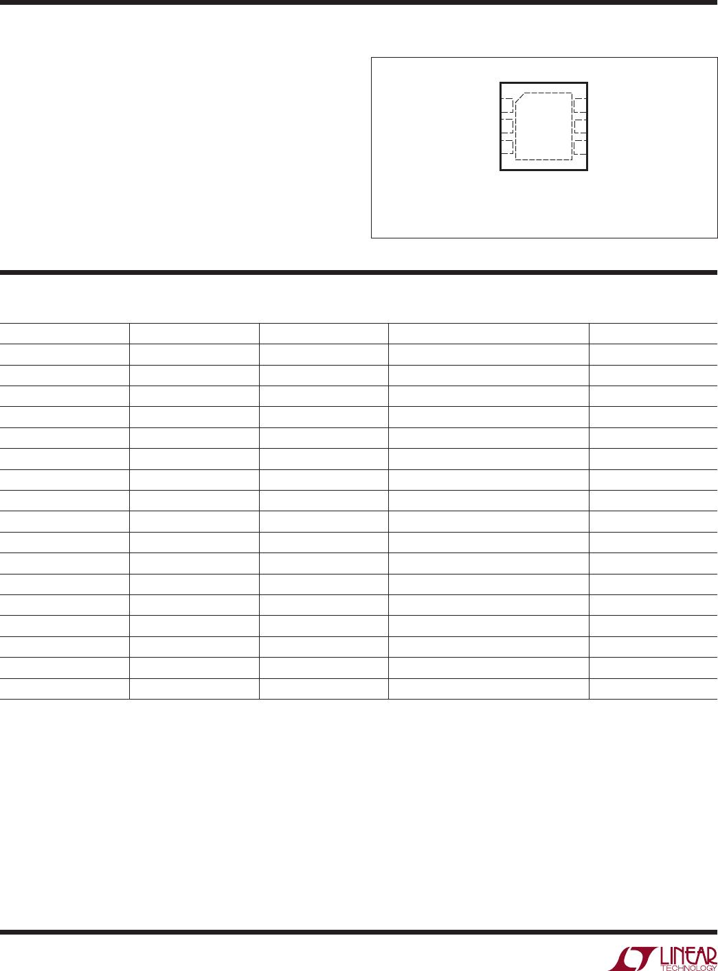
The LTC3025-X is available in a tiny, low profile (0.75mm)
6-lead DFN (2mm × 2mm) package.
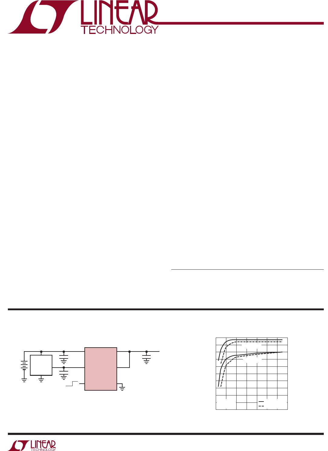
1.2V Output Voltage from 1.5V Input Supply
n
Wide Input Voltage Range: 0.9V to 5.5V
n
Stable with Ceramic Capacitors
n
Very Low Dropout: 85mV at 500mA
n
Adjustable Output Range: 0.4V to 3.6V (LTC3025-1)
n
Fixed Output: 1.2V (LTC3025-2), 1.5V (LTC3025-3),
1.8V (LTC3025-4)
n
±2% Voltage Accuracy over Temperature,
Supply and Load
n
Low Noise: 80µV
RMS
(10Hz to 100kHz)
n
BIAS Voltage Range: 2.5V to 5.5V
n
Fast Transient Recovery
n
Shutdown Disconnects Load from V
IN
and V
BIAS
n
Low Operating Current: I
IN
= 4µA, I
BIAS
= 50µA Typ
n
Low Shutdown Current: I
IN
= 1µA, I
BIAS
= 0.01µA Typ
n
Output Current Limit
n
Thermal Overload Protection
n
Available in 6-Lead (2mm × 2mm) DFN Package
n
Low Power Handheld Devices
n
Low Voltage Logic Supplies
n
DSP Power Supplies
n
Cellular Phones
n
Portable Electronic Equipment
n
Handheld Medical Instruments
n
Post Regulator for Switching Supply Noise Rejection
1MHz V
IN
Supply Rejection
LTC3025-2
BIAS
0.1µF
1.5V
1µF
0.1µF
Li-Ion
OR
3-CELL
NiMH
IN
SHDN
OUT
V
OUT
= 1.2V
I
OUT
≤ 500mA
30251234 TA01
SENSE
GNDOFF ON
1.5V HIGH
EFFICIENCY
DC/DC
BUCK
V
IN
(V)
1.2
0
REJECTION (dB)
5
15
20
25
50
35
1.6
2.0
2.2
30251234 TA01b
10
40
45
30
1.4
1.8
2.4
2.6
BIAS = 3.6V
V
OUT
= 1.2V
I
OUT
= 100mA
I
OUT
= 300mA
C
OUT
= 1µF
C
OUT
= 10µF
L, LT, LTC, LTM, Linear Technology and the Linear logo are registered trademarks and VLDO
and ThinSOT are trademarks of Linear Technology Corporation. All other trademarks are the
property of their respective owners. Protected by U.S. Patents including 7224204, 7218082.
LTC3025-1/LTC3025-2/
LTC3025-3/LTC3025-4
2
30251234ff
pin conFiguraTionabsoluTe MaxiMuM raTings
V
BIAS
, V
IN
to GND ......................................... –0.3V to 6V
SHDN to GND ............................................... –0.3V to 6V
SENSE, ADJ to GND ..................................... –0.3V to 6V
V
OUT
........................................ –0.3V to V
IN
+ 0.3V or 6V
Operating Junction Temperature Range
(Note 3) .................................................. –40°C to 125°C
Storage Temperature Range ................... –65°C to 125°C
Output Short-Circuit Duration .......................... Indefinite
(Notes 1, 2)
TOP VIEW
7
DC6 PACKAGE
6-LEAD (2mm × 2mm) PLASTIC DFN
4
5
6
3
2
1BIAS
GND
IN
SHDN
ADJ/SENSE*
OUT
T
JMAX
= 125°C, θ
JA
= 102°C/W, θ
JC
= 20°C/W
EXPOSED PAD (PIN 7) IS GND, MUST BE SOLDERED TO PCB
*ADJ FOR LTC3025-1, SENSE FOR LTC3025-2, LTC3025-3, LTC3025-4
orDer inForMaTion
LEAD FREE FINISH TAPE AND REEL PART MARKING* PACKAGE DESCRIPTION TEMPERATURE RANGE
LTC3025EDC-1#PBF LTC3025EDC-1#TRPBF LDDW 6-Lead (2mm × 2mm) Plastic DFN –40°C to 125°C
LTC3025IDC-1#PBF LTC3025IDC-1#TRPBF LDDW 6-Lead (2mm × 2mm) Plastic DFN –40°C to 125°C
LTC3025EDC-2#PBF LTC3025EDC-2#TRPBF LDMK 6-Lead (2mm × 2mm) Plastic DFN –40°C to 125°C
LTC3025IDC-2#PBF LTC3025IDC-2#TRPBF LDMK 6-Lead (2mm × 2mm) Plastic DFN –40°C to 125°C
LTC3025EDC-3#PBF LTC3025EDC-3#TRPBF LDQS 6-Lead (2mm × 2mm) Plastic DFN –40°C to 125°C
LTC3025IDC-3#PBF LTC3025IDC-3#TRPBF LDQS 6-Lead (2mm × 2mm) Plastic DFN –40°C to 125°C
LTC3025EDC-4#PBF LTC3025EDC-4#TRPBF LDPQ 6-Lead (2mm × 2mm) Plastic DFN –40°C to 125°C
LTC3025IDC-4#PBF LTC3025IDC-4#TRPBF LDPQ 6-Lead (2mm × 2mm) Plastic DFN –40°C to 125°C
LEAD BASED FINISH TAPE AND REEL PART MARKING* PACKAGE DESCRIPTION TEMPERATURE RANGE
LTC3025EDC-1 LTC3025EDC-1#TR LDDW 6-Lead (2mm × 2mm) Plastic DFN –40°C to 125°C
LTC3025IDC-1 LTC3025IDC-1#TR LDDW 6-Lead (2mm × 2mm) Plastic DFN –40°C to 125°C
LTC3025EDC-2 LTC3025EDC-2#TR LDMK 6-Lead (2mm × 2mm) Plastic DFN –40°C to 125°C
LTC3025IDC-2 LTC3025IDC-2#TR LDMK 6-Lead (2mm × 2mm) Plastic DFN –40°C to 125°C
LTC3025EDC-3 LTC3025EDC-3#TR LDQS 6-Lead (2mm × 2mm) Plastic DFN –40°C to 125°C
LTC3025IDC-3 LTC3025IDC-3#TR LDQS 6-Lead (2mm × 2mm) Plastic DFN –40°C to 125°C
LTC3025EDC-4 LTC3025EDC-4#TR LDPQ 6-Lead (2mm × 2mm) Plastic DFN –40°C to 125°C
LTC3025IDC-4 LTC3025IDC-4#TR LDPQ 6-Lead (2mm × 2mm) Plastic DFN –40°C to 125°C
Consult LTC Marketing for parts specified with wider operating temperature ranges. *The temperature grade is identified by a label on the shipping container.
For more information on lead free part marking, go to: http://www.linear.com/leadfree/
For more information on tape and reel specifications, go to: http://www.linear.com/tapeandreel/
LTC3025-1/LTC3025-2/
LTC3025-3/LTC3025-4
3
30251234ff
elecTrical characTerisTics
The l denotes the specifications which apply over the full operating
temperature range, otherwise specifications are at T
A
= 25°C. V
IN
= 1.5V, V
BIAS
= 3.6V, C
OUT
= 1µF, C
IN
= 0.1µF, C
BIAS
= 0.1µF
(all capacitors ceramic) unless otherwise noted. (Note 3)
PARAMETER CONDITIONS MIN TYP MAX UNITS
V
IN
Operating Voltage (Note 4) LTC3025-1
l
0.9 5.5 V
LTC3025-2
l
1.4 5.5 V
LTC3025-3
l
1.7 5.5 V
LTC3025-4
l
2.0 5.5 V
V
BIAS
Operating Voltage (Note 4) LTC3025-1
l
2.5 5.5 V
LTC3025-2
l
2.7 5.5 V
LTC3025-3
l
3.0 5.5 V
LTC3025-4
l
3.3 5.5 V
V
BIAS
Undervoltage Lockout
l
2.2 2.5 V
V
IN
Operating Current I
OUT
= 10µA, V
OUT
= 1.2V, LTC3025-1
l
4 10 µA
V
IN
Operating Current I
OUT
= 0µA, LTC3025-2/LTC3025-3/LTC3025-4
l
4 10 µA
V
BIAS
Operating Current I
OUT
= 10µA, V
OUT
= 1.2V, LTC3025-1
l
50 80 µA
V
BIAS
Operating Current I
OUT
= 0µA, LTC3025-2/LTC3025-3/LTC3025-4
l
50 80 µA
V
IN
Shutdown Current V
SHDN
= 0V 1 5 µA
V
BIAS
Shutdown Current V
SHDN
= 0V 0.01 1 µA
V
ADJ
Regulation Voltage (Note 5) 1mA ≤ I
OUT
≤ 500mA, V
OUT
= 1.2V, 1.5V ≤ V
IN
≤ 5V, LTC3025-1
1mA ≤ I
OUT
≤ 500mA, V
OUT
= 1.2V, 1.5V ≤ V
IN
≤ 5V, LTC3025-1
l
0.395
0.392
0.4
0.4
0.405
0.408
V
V
V
SENSE
Regulation Voltage (Note 5) 1mA ≤ I
OUT
≤ 500mA, 1.5V ≤ V
IN
≤ 5V, LTC3025-2
1mA ≤ I
OUT
≤ 500mA, 1.5V ≤ V
IN
≤ 5V, LTC3025-2
l
1.185
1.176
1.2
1.2
1.215
1.224
V
V
V
SENSE
Regulation Voltage (Note 5) 1mA ≤ I
OUT
≤ 500mA, 1.7V ≤ V
IN
≤ 5V, LTC3025-3
1mA ≤ I
OUT
≤ 500mA, 1.7V ≤ V
IN
≤ 5V, LTC3025-3
l
1.481
1.470
1.5
1.5
1.519
1.530
V
V
V
SENSE
Regulation Voltage (Note 5) 1mA ≤ I
OUT
≤ 500mA, 2.0V ≤ V
IN
≤ 5V, LTC3025-4
1mA ≤ I
OUT
≤ 500mA, 2.0V ≤ V
IN
≤ 5V, LTC3025-4
l
1.777
1.764
1.8
1.8
1.823
1.836
V
V
I
ADJ
ADJ Input Current V
ADJ
= 0.45V, LTC3025-1 –50 0 50 nA
OUT Load Regulation (Referred to ADJ Pin) ∆I
OUT
= 1mA to 500mA, LTC3025-1 –0.35 mV
OUT Load Regulation ∆I
OUT
= 1mA to 500mA, LTC3025-2
∆I
OUT
= 1mA to 500mA, LTC3025-3
∆I
OUT
= 1mA to 500mA, LTC3025-4
–1
–1.3
–1.5
mV
mV
mV
V
IN
Line Regulation (Referred to ADJ Pin) V
IN
= 1.5V to 5V, V
BIAS
= 3.6V, V
OUT
= 1.2V,
I
OUT
= 1mA, LTC3025-1
0.07 mV
V
IN
Line Regulation V
IN
= 1.5V to 5V, V
BIAS
= 3.6V, I
OUT
= 1mA, LTC3025-2
V
IN
= 1.8V to 5V, V
BIAS
= 3.6V, I
OUT
= 1mA, LTC3025-3
V
IN
= 2.1V to 5V, V
BIAS
= 3.6V, I
OUT
= 1mA, LTC3025-4
0.21
0.26
0.32
mV
mV
mV
V
BIAS
Line Regulation V
IN
= 1.5V, V
BIAS
= 2.7V to 5V, V
OUT
= 1.2V, I
OUT
= 1mA,
LTC3025-1
l
4.5 16.5 mV
V
BIAS
Line Regulation V
IN
= 1.5V, V
BIAS
= 2.7V to 5V, I
OUT
= 1mA, LTC3025-2
V
IN
= 1.8V, V
BIAS
= 3.0V to 5V, I
OUT
= 1mA, LTC3025-3
V
IN
= 2.1V, V
BIAS
= 3.3V to 5V, I
OUT
= 1mA, LTC3025-4
l
l
l
4.5
4.5
4.5
16.5
16.5
16.5
mV
mV
mV
V
IN
to V
OUT
Dropout Voltage (Notes 4, 6) V
BIAS
= 3V, V
IN
= 1.5V, I
OUT
= 500mA,
V
ADJ
= 0.37V(LTC3025-1), V
SENSE
= 1.15V(LTC3025-2)
l
85 120
170
mV
mV
V
IN
to V
OUT
Dropout Voltage (Notes 4, 6) V
BIAS
= 3.1V, V
IN
= 1.7V, I
OUT
= 500mA,
V
SENSE
= 1.45V(LTC3025-3)
l
90 130
185
mV
mV
V
IN
to V
OUT
Dropout Voltage (Notes 4, 6) V
BIAS
= 3.4V, V
IN
= 2.0V, I
OUT
= 500mA,
V
SENSE
= 1.75V(LTC3025-4)
l
90 130
185
mV
mV
V
BIAS
to V
OUT
Dropout Voltage (Note 4) LTC3025-1
l
1.5 V

LTC3025EDC-3#TRPBF

Mfr. #:
Manufacturer:
Analog Devices / Linear Technology
Description:
LDO Voltage Regulators 1.5V, 500 mA Micropower, VLDO Linear Regulator
Lifecycle:
New from this manufacturer.
Delivery:
DHL FedEx Ups TNT EMS
Payment:
T/T Paypal Visa MoneyGram Western Union