LTC3025EDC-3#TRPBF

LTC3025-1/LTC3025-2/
LTC3025-3/LTC3025-4
7
30251234ff
pin FuncTions
BIAS (Pin 1): BIAS Input Voltage. BIAS provides internal
power for LTC3025-X circuitry. The BIAS pin should be
locally bypassed to ground if the LTC3025-X is more than a
few inches away from another source of bulk capacitance.
In general, the output impedance of a battery rises with
frequency, so it is usually advisable to include an input
bypass capacitor in battery-powered circuits. A capacitor
in the range of 0.01µF to 0.1µF is usually sufficient.
GND (Pin 2): Ground. Connect to a ground plane.
IN (Pin 3): Input Supply Voltage. The output load current
is supplied directly from IN. The IN pin should be locally
bypassed to ground if the LTC3025-X is more than a few
inches away from another source of bulk capacitance.
In general, the output impedance of a battery rises with
frequency, so it is usually advisable to include an input
bypass capacitor when supplying IN from a battery. A
capacitor in the range of 0.1µF to 1µF is usually sufficient.
OUT (Pin 4): Regulated Output Voltage. The OUT pin
supplies power to the load. A minimum ceramic output
capacitor of at least 1µF is required to ensure stability.
Larger output capacitors may be required for applications
with large transient loads to limit peak voltage transients.
See the Applications Information section for more informa-
tion on output capacitance.
ADJ (Pin 5) LTC3025-1: Adjust Input. This is the input to
the error amplifier. The ADJ pin reference voltage is 0.4V
referenced to ground. The output voltage range is 0.4V to
3.6V and is typically set by connecting ADJ to a resistor
divider from OUT to GND. See Figure 2.
SENSE (Pin 5) LTC3025-2, LTC3025-3, LTC3025-4: Output
Sense. The sense is the input to the resistor divider driving
the error amplifier. Optimum regulation will be obtained at
the point where SENSE is connected to OUT. The SENSE pin
bias current is 10µA at the nominal rated output voltage.
SHDN (Pin 6): Shutdown Input, Active Low. This pin is
used to put the LTC3025-X into shutdown. The SHDN pin
current is typically less than 10nA. The SHDN pin cannot
be left floating and must be tied to a valid logic level (such
as BIAS) if not used.
GND (Exposed Pad Pin 7): Ground and Heat Sink. Must
be soldered to PCB ground plane or large pad for optimal
thermal performance.
block DiagraM
3
1
6
2
4
5
IN
OUT
6µA
ADJ
GND
SHDN
BIAS
REFERENCE
SHDN 0.4V
SOFT-START
+
3
1
6
2
4
5
IN
OUT
6µA
30251234 BD
SENSE
GND
SHDN
BIAS
REFERENCE
SHDN 0.4V
SOFT-START
+
R1
40k
R2
80k (LTC3025-2)
110k (LTC3025-3)
140k (LTC3025-4)
LTC3025-1 LTC3025-2, LTC3025-3, LTC3025-4
LTC3025-1/LTC3025-2/
LTC3025-3/LTC3025-4
8
30251234ff
applicaTions inForMaTion
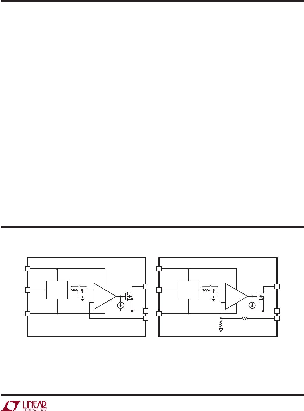
Operation (Refer to Block Diagram)
The LTC3025-X is a micropower, VLDO (very low dropout)
linear regulator which operates from input voltages as low
as 0.9V. The device provides a highly accurate output that
is capable of supplying 500mA of output current with a
typical dropout voltage of only 85mV. A single ceramic
capacitor as small as 1µF is all that is required for output
bypassing. A low reference voltage allows the LTC3025-1
output to be programmed to much lower voltages than
available in common LDOs (range of 0.4V to 3. 6V). The
LTC3025-2/LTC3025-3/LTC3025-4 have fixed outputs of
1.2V, 1.5V and 1.8V respectively, eliminating the need for
an external resistor divider.
As shown in the Block Diagram, the BIAS input supplies
the internal reference and LDO circuitry while all output
current comes directly from the IN input for high efficiency
regulation. The low quiescent supply currents I
IN
= 4µA,
I
BIAS
= 50µA drop to I
IN
= 1µA, I
BIAS
= 0.01µA typical in
shutdown making the LTC3025-X an ideal choice for use
in battery-powered systems.
The device includes current limit and thermal overload
protection. The fast transient response of the follower
output stage overcomes the traditional tradeoff between
dropout voltage, quiescent current and load transient
response inherent in most LDO regulator architectures.
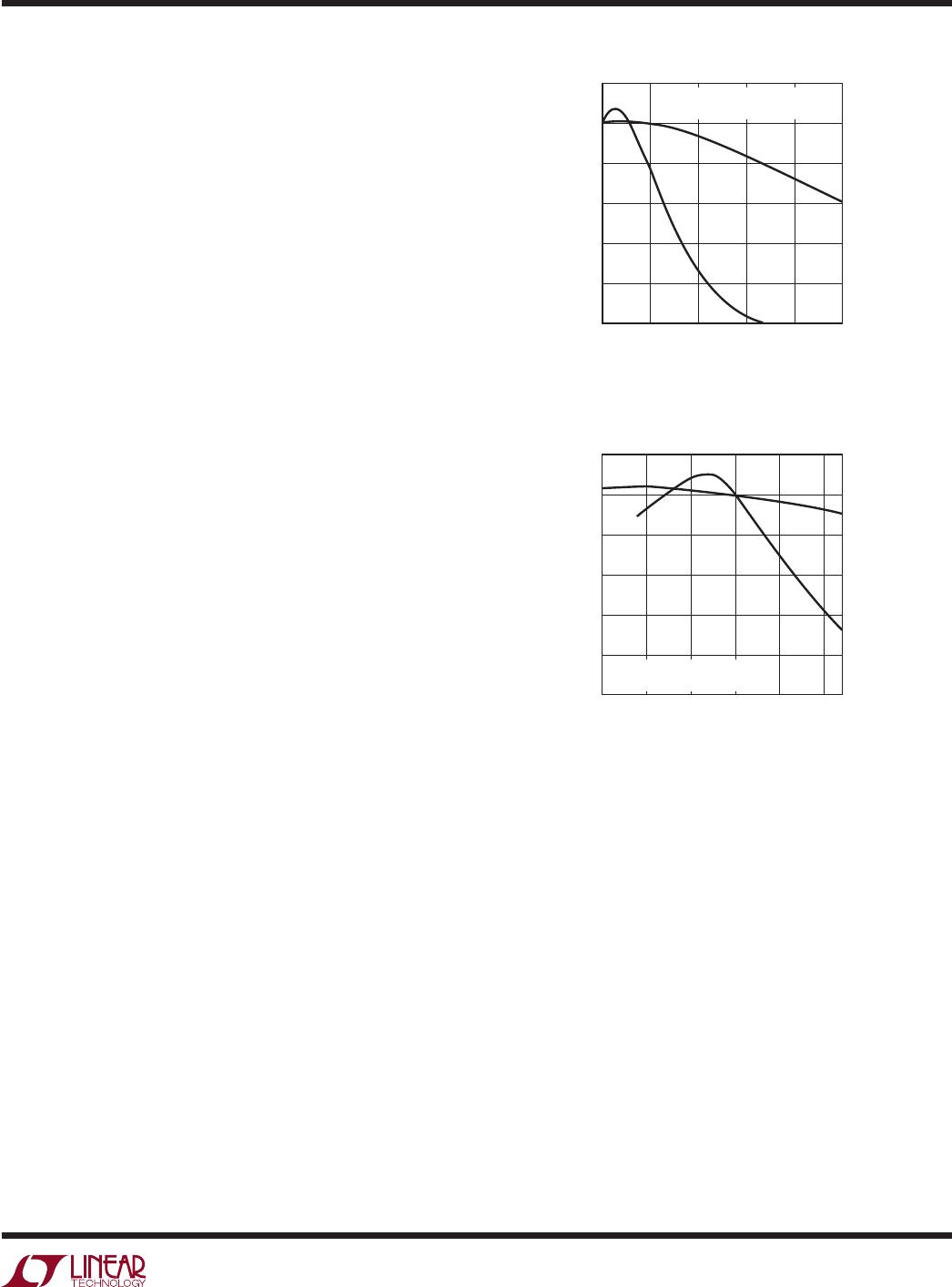
The LTC3025-X also includes overshoot detection circuitry
which brings the output back into regulation when going
from heavy to light output loads (see Figure 1).
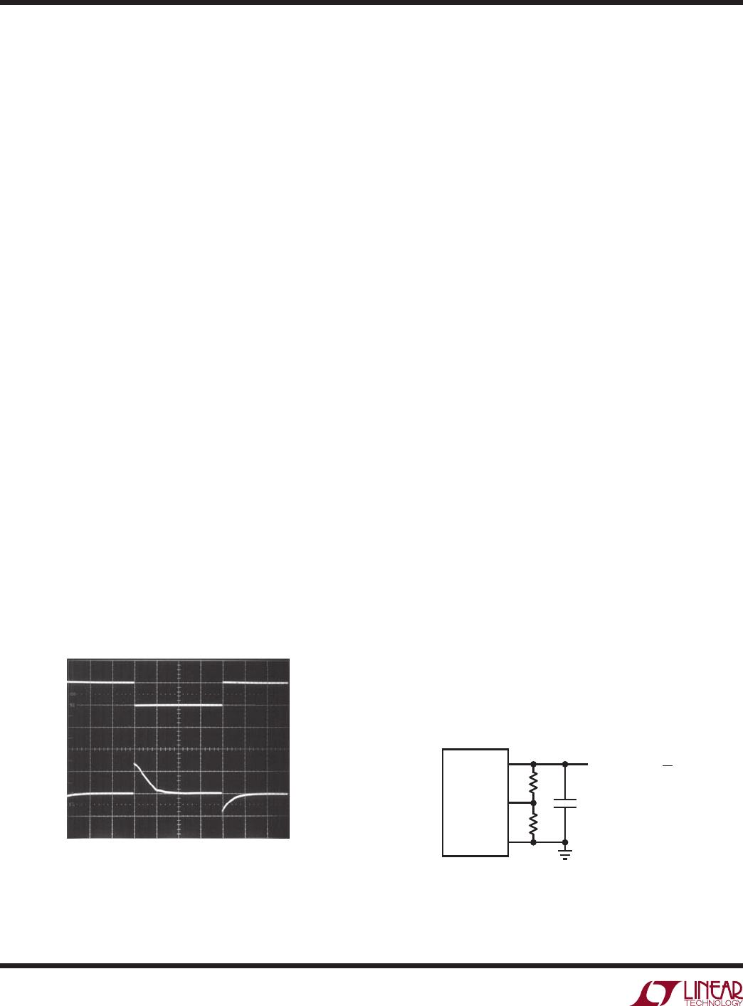
Figure 1. LTC3025-X Transient Response
300mA
0mA
I
OUT
V
OUT
AC
20mV/DIV
V
IN
= 1.5V
V
OUT
= 1.2V
V
BIAS
= 3.6V
C
OUT
= 1µF
100µs/DIV
30251234 F01
Adjustable Output Voltage (LTC3025-1)
The output voltage is set by the ratio of two external resis-
tors as shown in Figure 2. The device servos the output
to maintain the ADJ pin voltage at 0.4V (referenced to
ground). Thus, the current in R1 is equal to 0.4V/R1. For
good transient response, stability, and accuracy, the current
in R1 should be at least 8µA, thus the value of R1 should
be no greater than 50k. The current in R2 is the current in
R1 plus the ADJ pin bias current. Since the ADJ pin bias
current is typically <10nA, it can be ignored in the output
voltage calculation. The output voltage can be calculated
using the formula in Figure 2. Note that in shutdown the
output is turned off and the divider current will be zero
once C
OUT
is discharged.
The LTC3025-1 operates at a relatively high gain of –0.7µV/
mA referred to the ADJ input. Thus a load current change
of 1mA to 500mA produces a –0.35mV drop at the ADJ
input. To calculate the change referred to the output
simply multiply by the gain of the feedback network
(i. e. ,1 + R2/R1). For example, to program the output for
1.2V choose R2/R1 = 2. In this example, an output current
change of 1mA to 500mA produces –0.35mV • (1 + 2) =
1.05mV drop at the output.
Because the ADJ pin is relatively high impedance (depend-
ing on the resistor divider used), stray capacitance at this
pin should be minimized (<10pF) to prevent phase shift
in the error amplifier loop. Additionally, special attention
should be given to any stray capacitances that can couple
external signals onto the ADJ pin producing undesirable
output ripple. For optimum performance connect the ADJ
pin to R1 and R2 with a short PCB trace and minimize all
other stray capacitance to the ADJ pin.
Figure 2. Programming the LTC3025-1
( )
OUT
R1
R2
30251234 F02
C
OUT
R2
R1
V
OUT
= 0.4V 1 +
ADJ
GND
LTC3025-1/LTC3025-2/
LTC3025-3/LTC3025-4
9
30251234ff
applicaTions inForMaTion
Output Capacitance and Transient Response
The LTC3025-X is designed to be stable with a wide range
of ceramic output capacitors. The ESR of the output capaci-
tor affects stability, most notably with small capacitors. A
minimum output capacitor of 1µF with an ESR of 0.05Ω or
less is recommended to ensure stability. The LTC3025-X is
a micropower device and output transient response will be
a function of output capacitance. Larger values of output
capacitance decrease the peak deviations and provide im-
proved transient response for larger load current changes.
Note that bypass capacitors used to decouple individual
components powered by the LTC3025-X will increase the
effective output capacitor value. High ESR tantalum and
electrolytic capacitors may be used, but a low ESR ceramic
capacitor must be in parallel at the output. There is no
minimum ESR or maximum capacitor size requirements.
Extra consideration must be given to the use of ceramic
capacitors. Ceramic capacitors are manufactured with a
variety of dielectrics, each with different behavior across
temperature and applied voltage. The most common di-
electrics used are Z5U, Y5V, X5R and X7R. The Z5U and
Y5V dielectrics are good for providing high capacitances
in a small package, but exhibit large voltage and tem-
perature coefficients as shown in Figures 3 and 4. When
used with a 2V regulator, a 1µF Y5V capacitor can lose as
much as 75% of its initial capacitance over the operating
temperature range. The X5R and X7R dielectrics result in
more stable characteristics and are usually more suitable
for use as the output capacitor. The X7R type has better
stability across temperature, while the X5R is less expensive
and is available in higher values. In all cases, the output
capacitance should never drop below 0.4µF, or instability
or degraded performance may occur.
Figure 3. Ceramic Capacitor DC Bias Characteristics
Figure 4. Ceramic Capacitor Temperature Characteristics
DC BIAS VOLTAGE (V)
CHANGE IN VALUE (%)
30251234 F03
20
0
–20
–40
–60
–80
–100
0
4
8
10
2 6
X5R
Y5V
BOTH CAPACITORS ARE 1µF,
10V, 0603 CASE SIZE
TEMPERATURE (°C)
–50
–100
CHANGE IN VALUE (%)
–80
–60
–40
–20
X5R
Y5V
20
–25
0 25 50
30251234 F04
75
0
BOTH CAPACITORS ARE 1µF,
10V, 0603 CASE SIZE

LTC3025EDC-3#TRPBF

Mfr. #:
Manufacturer:
Analog Devices / Linear Technology
Description:
LDO Voltage Regulators 1.5V, 500 mA Micropower, VLDO Linear Regulator
Lifecycle:
New from this manufacturer.
Delivery:
DHL FedEx Ups TNT EMS
Payment:
T/T Paypal Visa MoneyGram Western Union