LTC3025-1/LTC3025-2/
LTC3025-3/LTC3025-4
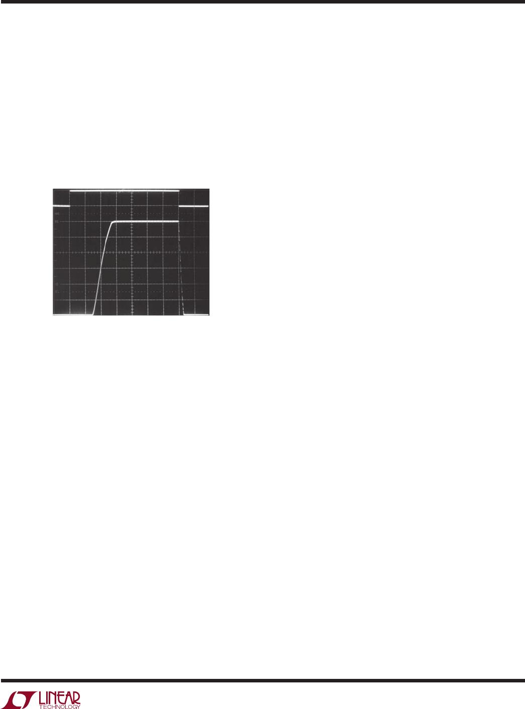
10
30251234ff
applicaTions inForMaTion
Thermal Considerations
The power handling capability of the device will be limited
by the maximum rated junction temperature (125°C). The
power dissipated by the device will be the output current
multiplied by the input/output voltage differential:
(I
OUT
) (V
IN
– V
OUT
)
Note that the BIAS current is less than 500µA even under
heavy loads, so its power consumption can be ignored
for thermal calculations.
The LTC3025-X has internal thermal limiting designed to
protect the device during momentary overload conditions.
For continuous normal conditions, the maximum junction
temperature rating of 125°C must not be exceeded. It is
important to give careful consideration to all sources of
thermal resistance from junction to ambient. Additional
heat sources mounted nearby must also be considered.
For surface mount devices, heat sinking is accomplished
by using the heat-spreading capabilities of the PC board
and its copper traces. Copper board stiffeners and plated
through holes can also be used to spread the heat gener-
ated by power devices.
The LTC3025-X 2mm × 2mm DFN package is specified
as having a junction-to-ambient thermal resistance of
102°C/W, which assumes a minimal heat spreading cop-
per plane. The actual thermal resistance can be reduced
substantially by connecting the package directly to a good
heat spreading ground plane. When soldered to 2500mm
2
double-sided 1 oz. copper plane, the actual junction-to-
ambient thermal resistance can be less than 60°C/W.
Calculating Junction Temperature
Example: Given an output voltage of 1.2V, an input voltage
of 1.8V to 3V, an output current range of 0mA to 100mA
and a maximum ambient temperature of 50°C, what will
the maximum junction temperature be?
The power dissipated by the device will be equal to:
I
OUT(MAX)
(V
IN(MAX)
– V
OUT
)
where:
I
OUT(MAX)
= 100mA
V
IN(MAX)
= 3V
So:
P = 100mA(3V – 1.2V) = 0.18W
Even under worst-case conditions, the LTC3025-X’s BIAS
pin power dissipation is only about 1mW, thus can be ig-
nored. Assuming a junction-to-ambient thermal resistance
of 102°C/W, the junction temperature rise above ambient
will be approximately equal to:
0.18W(102°C/W) = 18.4°C
The maximum junction temperature will then be equal to
the maximum junction temperature rise above ambient
plus the maximum ambient temperature or:
T
J
= 50°C + 18.4°C = 68.4°C
Short-Circuit/Thermal Protection
The LTC3025-X has built-in short-circuit current limiting
as well as overtemperature protection. During short-circuit
conditions, internal circuitry automatically limits the output
current to approximately 1130mA. At higher temperatures,
or in cases where internal power dissipation causes exces-
sive self heating on chip, the thermal shutdown circuitry
will shut down the LDO when the junction temperature
exceeds approximately 150°C. It will re enable the LDO
once the junction temperature drops back to approximately
140°C. The LTC3025-X will cycle in and out of thermal
shutdown without latch-up or damage until the overstress
condition is removed. Long term overstress (T
J
> 125°C)
should be avoided as it can degrade the performance or
shorten the life of the part.