LTC4151
13
4151ff
For more information www.linear.com/LTC4151
address with the R/W bit now set to one. The LTC4151
acknowledges and sends the contents of the requested
register. The transmission terminates when the master
sends a Stop condition. If the master acknowledges the
transmitted data byte, as in a Read Word command, the
LTC4151 will send the contents of the next register. If
the master acknowledges the second data byte and each
of the following (if more) data bytes, as in a Read Page
command, the LTC4151 will keep sending out each data
byte in the register that corresponds to the incrementing
register pointer. The read operation terminates and the
register address pointer resets to 00h when the master
sends a Stop condition.
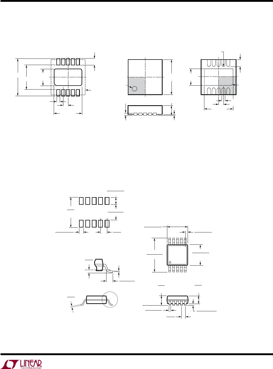
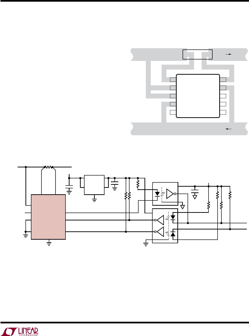
Layout Considerations
A Kelvin connection between the sense resistor R
S
and
the LTC4151 is recommended to achieve accurate cur-
rent
sensing (
Figure 10). The minimum trace width for
1oz copper foil is 0.02" per amp to make sure the trace
applicaTions inForMaTion
4151 F10
SENSE
GND
SENSE
+
V
IN
ADR1
ADR0
LTC4151
V
IN
GND
R
S
I
LOAD
I
LOAD
Figure 10. Recommended Layout for Kelvin Connection
stays at a reasonable temperature. Using 0.03" per amp
or wider is recommended. Note that 1oz copper exhibits
a sheet resistance of about 530µW per square.
ADINADIN
R1
0.02Ω
LTC4151-2
V
IN
7V TO 80V
V
OUT
V
CC
8
5V
1
2
8
7
6
5
1
2
3
4
ISO_SDA
ISO_SCL
7
5
GND
4
1
2
8
5
C7
F
100V
V
IN
V
IN
ADR1
ADR0
SDAO
IN
LT3010-5
SHDN
OUT
SENSE
GND
SDAI
SCL
GND
SENSE
+
SENSE
C6
F
ISO1
PS9817-2
ISO2
PS9817-2
R3
10k
R4
10k
R11
1k
R13
10k
4151 F11
R12
1k
R14
10k
R8
1k
C4
0.1µF
V
CC
GND
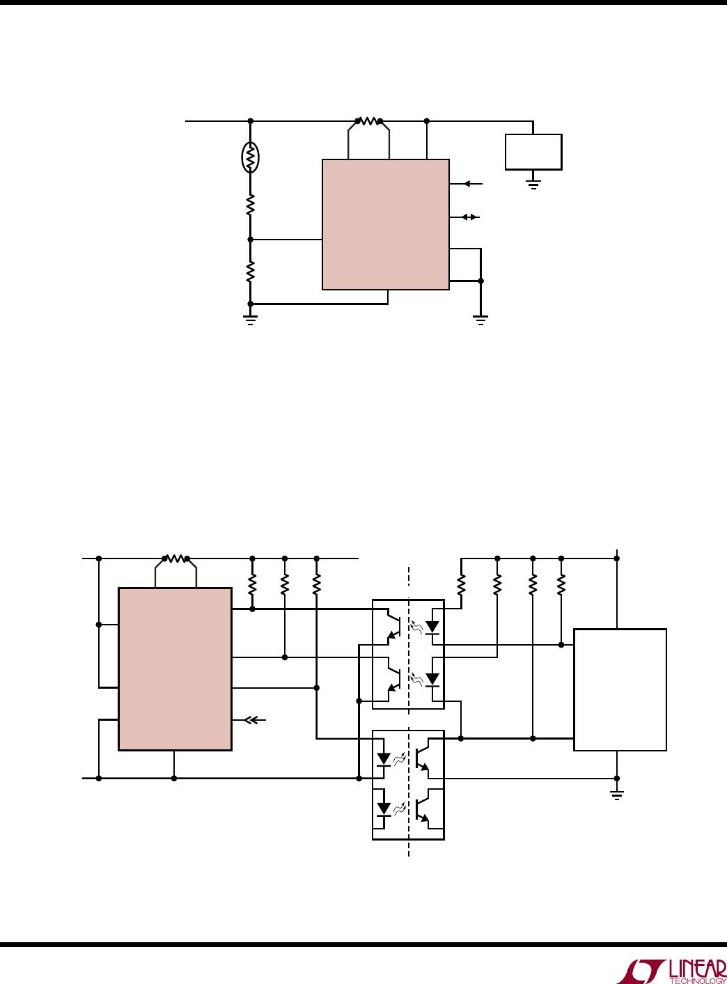
Figure 11. LTC4151-2 I
2
C Opto-Isolation Interface with High Speed Opto-Couplers
LTC4151
14
4151ff
For more information www.linear.com/LTC4151
Typical applicaTion
LTC4151
SCL
V
IN
48V
V
IN
SENSE
+
SENSE
0.2Ω
I
2
C
SDA
ADR1
ADR0
ADIN
40.2k
1%
100k AT 25°C
1%
1.5k
1%
VISHAY
2381 615 4.104
250mA
LOAD
GND
4151 TA02
Temperature Monitoring with an NTC Thermistor While
Measuring Load Current and LTC4151 Supply Current
T(°C) = 58.82 • (N
ADIN
/N
VIN
– 0.1066), 20°C < T < 60°C.
N
ADIN
AND N
VIN
ARE DIGITAL CODES MEASURED BY THE
ADC AT THE ADIN AND V
IN
PINS, RESPECTIVELY.
LTC4151-1 Monitors Current and Input Voltage of a –48V System and Interfaces with
a Microcontroller (1.5kHz Data Rate of I
2
C is Limited by Slew Rate of Opto-Isolators)
4151 TA04
3.3V
R
S
0.02Ω
µ-CONTROLLER
GND
LTC4151-1
SCL
SCL
RTN
–48V
V
IN
V
DD
V
ADIN
SDAI
ADIN
ADR1
R5
0.51k
R6
10k
R7
10k
R4
0.51k
R1
20k
R2
20k
R3
5.1k
18
27
36
45
81
72
63
54
SDA
ADR0
GND
SENSE
+
SENSE
SDA0
MOCD207M
MOCD207M
LTC4151
15
4151ff
For more information www.linear.com/LTC4151
DD Package
10-Lead Plastic DFN (3mm × 3mm)
(Reference LTC DWG # 05-08-1699 Rev C)
3.00 ±0.10
(4 SIDES)
NOTE:
1. DRAWING TO BE MADE A JEDEC PACKAGE OUTLINE M0-229 VARIATION OF (WEED-2).
CHECK THE LTC WEBSITE DATA SHEET FOR CURRENT STATUS OF VARIATION ASSIGNMENT
2. DRAWING NOT TO SCALE
3. ALL DIMENSIONS ARE IN MILLIMETERS
4. DIMENSIONS OF EXPOSED PAD ON BOTTOM OF PACKAGE DO NOT INCLUDE
MOLD FLASH. MOLD FLASH, IF PRESENT, SHALL NOT EXCEED 0.15mm ON ANY SIDE
5. EXPOSED PAD SHALL BE SOLDER PLATED
6. SHADED AREA IS ONLY A REFERENCE FOR PIN 1 LOCATION ON THE
TOP AND BOTTOM OF PACKAGE
0.40 ± 0.10
BOTTOM VIEW—EXPOSED PAD
1.65 ± 0.10
(2 SIDES)
0.75 ±0.05
R = 0.125
TYP
2.38 ±0.10
(2 SIDES)
15
106
PIN 1
TOP MARK
(SEE NOTE 6)
0.200 REF
0.00 – 0.05
(DD) DFN REV C 0310
0.25 ± 0.05
2.38 ±0.05
(2 SIDES)
RECOMMENDED SOLDER PAD PITCH AND DIMENSIONS
1.65 ±0.05
(2 SIDES)2.15 ±0.05
0.50
BSC
0.70 ±0.05
3.55
±0.05
PACKAGE
OUTLINE
0.25 ± 0.05
0.50 BSC
PIN 1 NOTCH
R = 0.20 OR
0.35 × 45°
CHAMFER
package DescripTion
Please refer to http://www.linear.com/designtools/packaging/ for the most recent package drawings.
MSOP (MS) 0213 REV F
0.53 ±0.152
(.021 ±.006)
SEATING
PLANE
0.18
(.007)
1.10
(.043)
MAX
0.17 –0.27
(.007 – .011)
TYP
0.86
(.034)
REF
0.50
(.0197)
BSC
1 2
3
4 5
4.90 ±0.152
(.193 ±.006)
0.497 ±0.076
(.0196 ±.003)
REF
8910
7
6
3.00 ±0.102
(.118 ±.004)
(NOTE 3)
3.00 ±0.102
(.118 ±.004)
(NOTE 4)
NOTE:
1. DIMENSIONS IN MILLIMETER/(INCH)
2. DRAWING NOT TO SCALE
3. DIMENSION DOES NOT INCLUDE MOLD FLASH, PROTRUSIONS OR GATE BURRS.
MOLD FLASH, PROTRUSIONS OR GATE BURRS SHALL NOT EXCEED 0.152mm (.006") PER SIDE
4. DIMENSION DOES NOT INCLUDE INTERLEAD FLASH OR PROTRUSIONS.
INTERLEAD FLASH OR PROTRUSIONS SHALL NOT EXCEED 0.152mm (.006") PER SIDE
5. LEAD COPLANARITY (BOTTOM OF LEADS AFTER FORMING) SHALL BE 0.102mm (.004") MAX
0.254
(.010)
0° – 6° TYP
DETAIL “A”
DETAIL “A”
GAUGE PLANE
5.10
(.201)
MIN
3.20 – 3.45
(.126 – .136)
0.889 ±0.127
(.035 ±.005)
RECOMMENDED SOLDER PAD LAYOUT
0.305 ±0.038
(.0120 ±.0015)
TYP
0.50
(.0197)
BSC
0.1016 ±0.0508
(.004 ±.002)
MS Package
10-Lead Plastic MSOP
(Reference LTC DWG # 05-08-1661 Rev F)

LTC4151CS-2#TRPBF

Mfr. #:
Manufacturer:
Analog Devices Inc.
Description:
Current & Power Monitors & Regulators 80V HIgh-Side Power Monitor with Shutdown
Lifecycle:
New from this manufacturer.
Delivery:
DHL FedEx Ups TNT EMS
Payment:
T/T Paypal Visa MoneyGram Western Union