LTC4151
7
4151ff
For more information www.linear.com/LTC4151
block DiagraM
operaTion
The LTC4151 accurately monitors high side current and
voltages. This device accepts a wide range of input volt-
ages from
as low as 7V up to 80V and consumes less
than
1.7mA quiescent current in normal operation. A
shutdown mode is available with the LTC4151 to reduce
the quiescent current to less than 300µA by pulling the
SHDN pin below 1V.
In default continuous scan mode after power-up, the
onboard 12-bit analog-to-digital converter (ADC) continu
-
ously and sequentially measures the high side differential
voltage
between SENSE
+
(Kelvin sense of V
IN
) and SENSE
(full-scale 81.92mV) through an internal sense amplifier,
the input voltage V
IN
(full-scale 102.4V) through an internal
voltage divider, and the voltage applied to the ADIN pin
(full-scale 2.048V). The reference voltage of the ADC is
internally set to 2.048V. The digital data obtained by the
ADC is stored in the onboard registers.
In snapshot mode, the LTC4151 can perform on-demand
measurement of a selected voltage without the need of
continuous polling by a master controller. The snapshot
mode is enabled by programming the control register
through the I
2
C interface. A status bit in the data register
monitors the ADC’s conversion. When the conversion is
completed, the 12-bit digital code of the measured voltage
is held in the corresponding data registers.
The LTC4151 provides an I
2
C interface to read the ADC
data from the data registers and to program the control
register. Tw o three-state pins, ADR0 and ADR1, are
used to decode nine device addresses (see Table 1). The
LTC4151 features a single SDA pin to handle both input
data and output data, while the LTC4151-1/LTC4151-2
provide separate data in (SDAI) and data out (SDAO on
the LTC4151-1 and SDAO on the LTC4151-2) pins to
facilitate opto-isolation.
SHUTDOWN
CONTROL
4151 BD
6.3V
I
2
C/
REGISTERS
DECODER
SHDN
(LTC4151)
V
IN
5µA
2k
R
S
V
REF
= 2.048V
SDA/SDAI
(LTC4151/
LTC4151-1)
ADR1
SCL
SDAO/SDAO
(LTC4151-1/
LTC4151-2)
ADR0
GND ADIN
15k
735k
INTERNAL
POWER
SENSE
+
SENSE
+
6V
12-BIT ADC
MUX
25X
6V
pin FuncTions
SHDN (LTC4151 Only): Shutdown Input. Internally pulled
up to 6.3V. Pull this pin below 1V to force the LTC4151
into shutdown mode. Leave this pin open if unused.
V
IN
: Supply Voltage Input. Accepts 7V to 80V. The voltage
at this pin is monitored by the onboard ADC with a full-
scale input range of 102.4V. SENSE
+
must be connected
to V
IN
for proper ADC readout.
LTC4151
8
4151ff
For more information www.linear.com/LTC4151
applicaTions inForMaTion
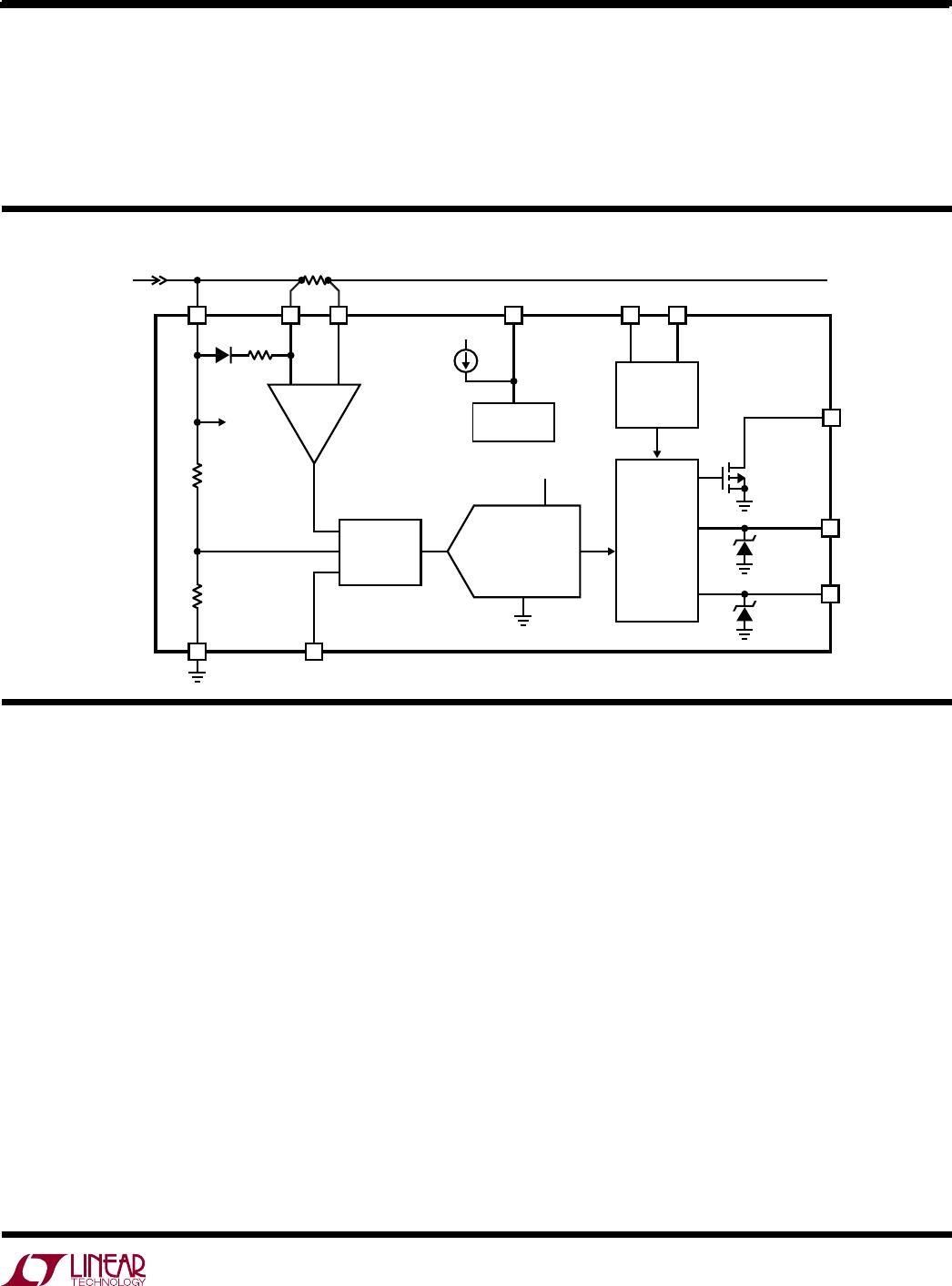
The LTC4151 offers a compact complete solution for high
side power monitoring. With a wide operating voltage
range from 7V to 80V, this device is ideal for a variety of
applications including consumer, automotive, industrial
and telecom infrastructure. The simple application circuit as
shown in Figure 1 provides monitoring of high side current
with a 0.02W resistor (4.096A in full scale), input voltage
(102.4V in full scale) and an external voltage (2.048V in
full scale), all with an internal 12-bit resolution ADC.
Data Converter
The LTC4151 features an onboard, 12-bit ∆Σ A/D
converter (ADC) that continuously monitors three volt
-
ages in the sequence of (V
SENSE
+
V
SENSE
) first, V
IN
second and V
ADIN
third. The ∆Σ architecture inherently
averages signal noise during the measurement period.
The differential voltage between SENSE
+
and SENSE
is
monitored with an 81.92mV full scale and 20µV resolu-
tion that
allows accurate measurement of the high side
input
current. SENSE
+
is a Kelvin sense pin for the V
IN
pin and must be connected to V
IN
(see Figure 10) for
proper ADC readout. The supply voltage at V
IN
is directly
measured with a 102.4V full scale and 25mV resolution.
The
voltage at the uncommitted ADIN pin is measured
with
a 2.048V full scale and 0.5mV resolution that allows
monitoring of any external voltage. The 12-bit digital
Figure 1. Monitoring High Side Current and Voltages Using the LTC4151
code of each measured voltage is stored in two adjacent
registers out
of the six total data registers A through F,
with the eight MSBs in the first register and the four LSBs
in the second (Table 2).
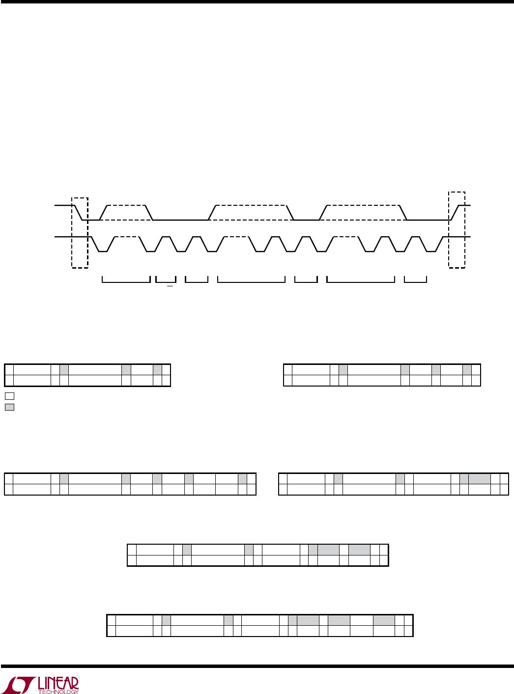
The data in registers A through F is refreshed at a frequency
of 7.5Hz in continuous scan mode. Setting control register
bit G4 (Table 6) invokes a test mode that halts updating
of these registers so that they can be written to and read
from for software testing.
The data converter features a snapshot mode allowing us
-
ers to make one-time measurements of a selected voltage
(either
the SENSE voltage, V
IN
voltage, or ADIN voltage).
To enable snapshot mode, set control register bit G7 and
write the 2-bit code of the desired ADC channel to G6
and G5 (Table 6) using a Write Byte command. When the
Write Byte command is completed, the ADC measures the
selected voltage and a Busy Bit in the LSB data register is
set to indicate that the data is not ready. After complet-
ing the conversion, the ADC is halted and the Busy Bit is
reset to indicate that the data is ready. To make another
measurement of the same voltage or to measure another
voltage, first disable the snapshot mode for the previous
measurement by clearing control bit G7, then re-enable the
snapshot mode and write the code of the desired voltage
according to the procedure described above. The Busy Bit
remains reset in the continuous scan mode.
4151 F01
0.02Ω
µ-CONTROLLER
GND
LTC4151
SHDN
V
IN
7V TO 80V
V
IN
V
DD
V
ADIN
SCL
SDA
ADIN
ADR1
SCL
SDA
ADR0
GND
SENSE
+
SENSE
3.3V
V
OUT
2k 2k
LTC4151
9
4151ff
For more information www.linear.com/LTC4151
SCL
SDA
START
CONDITION
STOP
CONDITION
ADDRESS R/W ACK DATA ACK DATA ACK
1 - 7 8 9
4151 F02
a6 - a0 b7 - b0 b7 - b0
1 - 7 8 9 1 - 7 8 9
P
S
Figure 2. General Data Transfer over I
2
C
I
2
C Interface
The LTC4151 features an I
2
C-compatible interface to
provide access to six ADC data registers and a control
register for monitoring the measured voltages. Figure 2
shows a general data transfer format using the I
2
C. The
LTC4151is a read-write slave device and supports SMBus
Read Byte, Write Byte, Read Word and Write Word com
-
mands. The device also supports Read Page and Write
Page
commands that allow one to read or write more than
two bytes of data. When using the Read Page and Write
Page commands, the host need only to issue an initial
register address and the internal register address pointer
automatically increments by 1 after each byte of data is read
or written. After the register address reaches 06h, it will
be reset to 00h and continue the increment. Upon a Stop
condition, the register address is reset to 00h. If desired,
the Read Page and Write Page support can be disabled by
clearing control register bit G3. The data formats for the
above commands are shown in Figures 3 to 8.
applicaTions inForMaTion
Figure 3. LTC4151 Serial Bus SDA Write Byte Protocol
Figure 4. LTC4151 Serial Bus SDA Write Word Protocol
Figure 5. LTC4151 Serial Bus SDA Write Page Protocol
S ADDRESS
1 1 0 a3:a0
FROM MASTER TO SLAVE
FROM SLAVE TO MASTER
A: ACKNOWLEDGE (LOW)
A: NOT ACKNOWLEDGE (HIGH)
R: READ BIT (HIGH)
COMMAND D ATA
X X X X X b2:b00
W
0 0 0b7:b0
A A A P
4151 F03
W: WRITE BIT (LOW)
S: START CONDITION
P: STOP CONDITION
S ADDRESS
1 1 0 a3:a0
COMMAND D ATA DATA
X X X X X b2:b00
W
0 0 0 0
4151 F04
b7:b0b7:b0
A
A A A P
S ADDRESS
1 1 0 a3:a0
COMMAND
0X X X X X b2:b00
W
0 0
4151 F05
A A A P
b7:b0
DATA
0
A
b7:b0
DATA
0
A
...
...
b7:b0
DATA
Figure 6. LTC4151 Serial Bus SDA Read Byte Protocol
S ADDRESS
1 1 0 a3:a0 1 1 0 a3:a0 1 0
COMMAND S ADDRESS R A
b7:b0 1
DATA
X X X X X b2:b00
W
0 0
4151 F06
A A A P
Figure 7. LTC4151 Serial Bus SDA Read Word Protocol
Figure 8. LTC4151 Serial Bus SDA Read Page Protocol
S ADDRESS
1 1 0 a3:a0 1 1 0 a3:a0 1 0
COMMAND S ADDRESS R A
b7:b0 1
DATA
X X X X X b2:b00
W
0 0
4151 F07
A
0
A
b7:b0
DATA
A A P
S ADDRESS
1 1 0 a3:a0 1 1 0 a3:a0 1 0
COMMAND S ADDRESS R A
b7:b0 1
DATA
X X X X X b2:b00
W
0 0
4151 F08
A
0
A
b7:b0
DATA
A A P
...
...
b7:b0
DATA

LTC4151CS-2#TRPBF

Mfr. #:
Manufacturer:
Analog Devices Inc.
Description:
Current & Power Monitors & Regulators 80V HIgh-Side Power Monitor with Shutdown
Lifecycle:
New from this manufacturer.
Delivery:
DHL FedEx Ups TNT EMS
Payment:
T/T Paypal Visa MoneyGram Western Union